Thermal infrared detector and infrared focal plane array

a detector and infrared technology, applied in the field of thermal infrared detectors, can solve the problems of limited size of each infrared detector, complicated device, and high cost of the whole device, and achieve the effect of reducing camera cost and pixel siz

Active Publication Date: 2006-02-28
MITSUBISHI ELECTRIC CORP
View PDF16 Cites 47 Cited by
  • Summary
  • Abstract
  • Description
  • Claims
  • Application Information

AI Technical Summary

Benefits of technology

[0014]However, with demands for high-resolution infrared focal plane arrays and reductions in camera costs, further reduction of the pixel size, i.e. the size of the thermal type infrared detectors is required.

Problems solved by technology

While the quantum type have an advantage in high sensitivity and rapid response, the entire device is complicated and costly since detectors need to be cooled to around −200° C. The thermal type exhibit inferior response speed, but they need not be cooled and may operate at room temperature.
In an infrared focal plane array in which such thermal type infrared detectors are arranged two-dimensionally as pixels, the size of each single infrared detector is limited.

Method used


Image

  • Thermal infrared detector and infrared focal plane array
  • Thermal infrared detector and infrared focal plane array
  • Thermal infrared detector and infrared focal plane array

Examples


embodiment 1

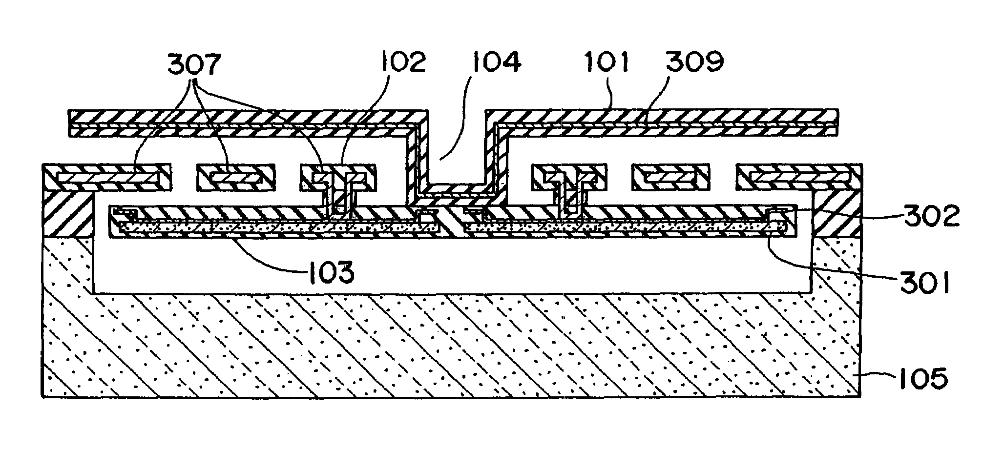
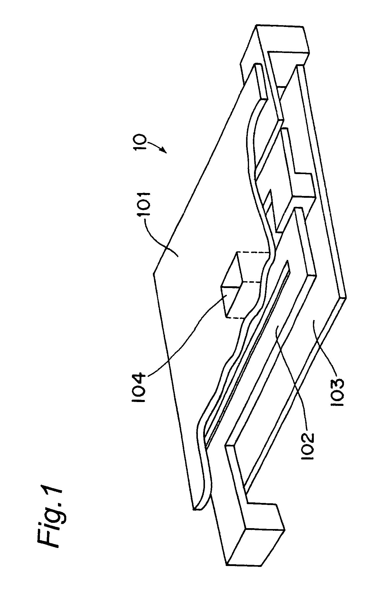
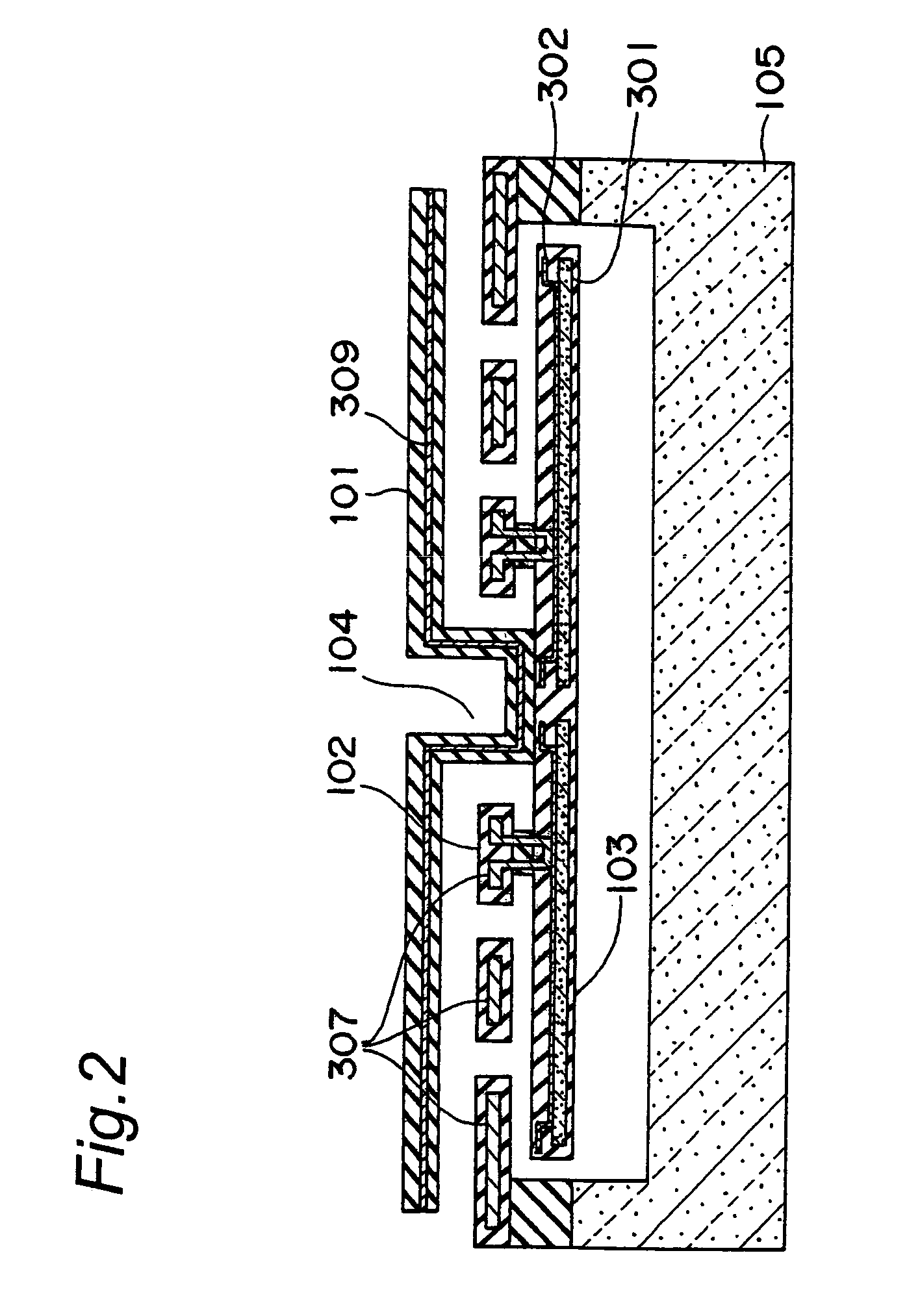
[0040]FIG. 1 is a perspective view illustrating a thermal type infrared detector according to a first embodiment of the present invention, and FIG. 2 is a schematic cross-sectional view thereof illustrating its cross-section in schematic form. The thermal type infrared detector 10 includes a substrate 105 of mono-crystalline silicon, a temperature sensor 103 which electric characteristics are changed in accordance with changes in temperature caused through infrared absorption, two heat-insulating supporting legs 102 for supporting the temperature sensor 103 in a heat-insulating manner and serving as signal lines for reading out electric signals from the temperature sensor 103, and an infrared absorption portion 101 formed to have thermal contact with the temperature sensor 103 via a supporting pillar 104. A portion of substrate 105 downward of the temperature sensor 103 is removed so as to form a cavity 107 so that the temperature sensor 103 is thermally insulated from the substrate...

embodiment 2

[0069]In embodiment 2, p-n junction diodes of vertical arrangement are employed as the temperature sensor 103. The remaining points are identical to those of Embodiment 1.

[0070]FIG. 8 is a plan view of a temperature sensor 103 employing p-n junction diodes of vertical arrangement, and FIG. 9 is a cross-sectional view seen from section A–A′ in FIG. 8. Similar to Embodiment 1, six p-n junction diodes 301(1) to 301. (6) (hereinafter generally referred to as “diodes 301”) are arranged in two rows, by threes on each side. The respective p-n junction diodes 301 are serially connected by using seven wiring electrodes 302(1) to 302(7) (hereinafter generally referred to as “wiring electrodes 302”). The fourth wiring electrode 302(4) is arranged in a crank-like manner that crosses the center of the rectangular detector for connecting the last diode 301(3) in the first row with the first diode 301(4) in the second row. The first wiring electrode 302(1) and the last wiring electrode 302(7) are ...

embodiment 3

[0072]In embodiment 3, Schottky diodes are used as the temperature sensor 103. The remaining points are identical to those of Embodiments 1 or 2.

[0073]FIG. 10 illustrates a cross-sectional view of the temperature sensor employing Schottky diodes. The arrangement of FIG. 10 corresponds to the p-n junction diodes as explained with reference to FIG. 9 in which the p-type regions 305 are not formed (in which no p-n junction is present). In the arrangement as illustrated in FIG. 10, upon suitably selecting a dopant density for an n-type silicon layer 801 and a material for the wiring electrodes 302 from among metal or metallic silicide, it is possible to form Schottky diodes on an interface between the n-type silicon layer 801 and the wiring electrodes 302. When a plurality of n-type silicon layers 801 are serially connected to the wiring electrodes 302, two interfaces 802 and 803 will be formed between the respective n-type silicon layers 801 and the wiring electrodes 302, each of which...


PUM


Abstract

A thermal infrared detector includes a substrate; a temperature sensor having electrical characteristics changed in accordance with changes in temperature caused by infrared absorption; heat-insulating supporting legs supporting and thermally insulating the temperature sensor and serving as signal lines for reading out electrical signals from the temperature sensor; and an infrared absorption layer in thermal contact the temperature sensor. Each of the temperature sensor, the heat-insulating supporting legs, and the infrared absorption layer is in a different plane and the planes are spatially separated from each other.

Description

BACKGROUND OF THE INVENTION[0001]1. Field of the Invention[0002]The present invention relates to a thermal infrared detector in which infrared rays are detected by conversion to heat and to an infrared focal plane array including such sensors aligned in a two-dimensional arrangement, and particularly to a structure of a thermal infrared detector detecting infrared rays with high sensitivity and low noise.[0003]2. Description of the Background Art[0004]Infrared focal plane arrays catch sight of objects that do not stimulate human sight and instantly measure temperatures of objects from distant places without contact. Such arrays are being used in diverse ways in a wide variety of industrial fields, for measuring and controlling manufacturing lines, as medical and diagnostic devices, and devices detecting humans. A general infrared focal plane array includes infrared detectors arranged in a two-dimensional matrix, and a signal read-out circuit around the array for reading signals from...

Claims


Application Information

Patent Timeline
Patent Type & Authority Patents(United States)
IPC IPC(8): G01J1/02G01J5/02G01J5/10G01J5/20G01J5/48H01L27/14H01L37/00
CPCG01J5/02G01J5/023G01J5/08H01L37/00G01J5/10H01L27/16G01J5/0853H10N19/00H10N15/00
Inventor ISHIKAWA, TOMOHIROUENO, MASASHI
Owner MITSUBISHI ELECTRIC CORP
Why Eureka
Try Eureka