Layered microelectronic contact and method for fabricating same

a micro-electronic contact and micro-electronic technology, applied in the direction of elastomeric connecting elements, printed element electric connection formation, dielectric characteristics, etc., can solve the problem that the cost of fabricating fine-pitch spring contacts has limited the range of applicability of fine-pitch spring contacts to less cost-sensitive applications, and the cost of manufacturing equipment and process time is associated with a large amount of fabrication cos

Inactive Publication Date: 2006-02-28
FORMFACTOR INC
View PDF27 Cites 25 Cited by
  • Summary
  • Abstract
  • Description
  • Claims
  • Application Information

AI Technical Summary

Benefits of technology

[0025]In another alternative embodiment, the traces are configured for a flip-chip application that requires no elastomer pad or underfill. The traces are shaped to be resilient in a direction parallel to the device substrate. For convenience, such traces are referred to herein as “horizontal springs,” and it should be apparent that “horizontal” is not limiting except in the sense of describing resiliency in the directio

Problems solved by technology

Once melted and re-hardened, the solder ball connections cannot readily be re-used, if at all.
Presently, however, the cost of fabricating fine-pitch spring contacts has limited their range of applicability to less cost-sensitive applications.
Much of the fabrication cost is associated with manufacturing equipment and process time.
One key disadvantage is the requirement for a polymer underfill beneath a die.
The presence of the underfill often makes it infeasible to rework the component.
This design lacks an elastomer layer for decoupling the die from the PCB and, therefore, may not eliminate the need for underfill.
The elastomeric materials tend to absorb moisture, and if excessive moisture is absorbed, rapid outgassing of this moisture at reflow temperatures may cause the formation of voids in the elastomer layer, or bursting of the package.
For

Method used


Image

  • Layered microelectronic contact and method for fabricating same
  • Layered microelectronic contact and method for fabricating same
  • Layered microelectronic contact and method for fabricating same

Examples


Embodiment Construction

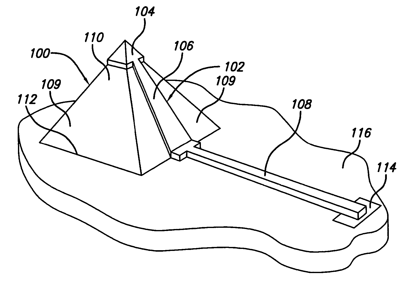
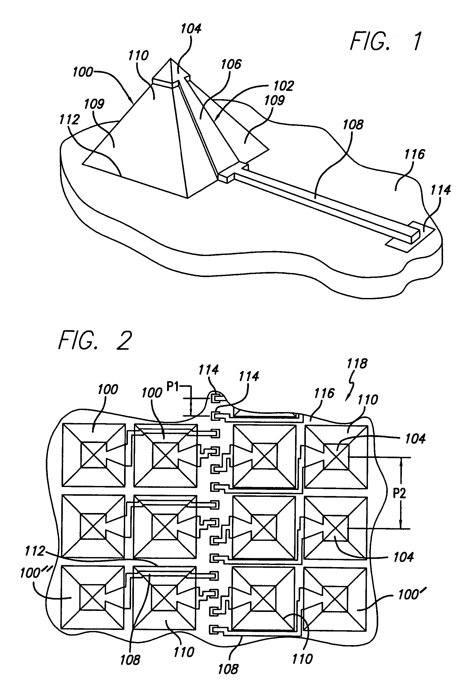
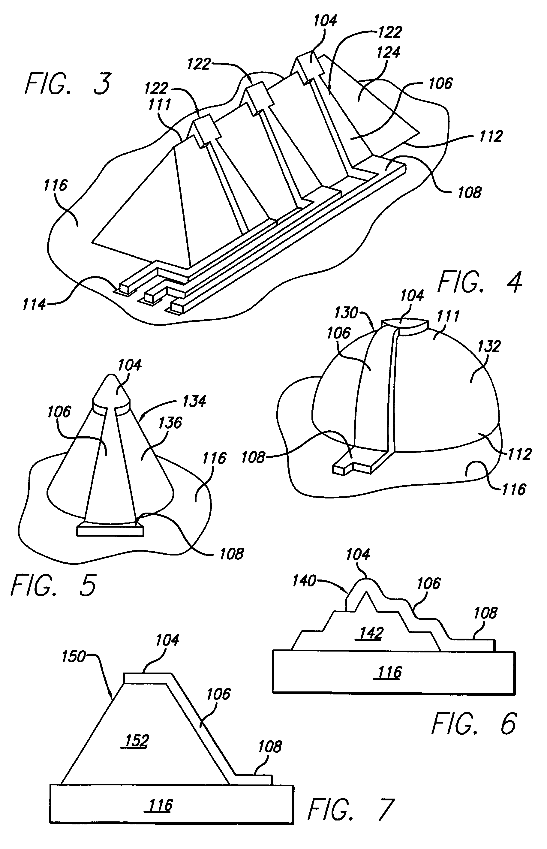
[0055]The present invention provides microelectronic spring contacts that overcome limitations of prior art spring contacts. In the detailed description that follows, like element numerals are used to describe like elements appearing in one or more of the figures.

[0056]The present invention achieves the benefits of multi-layer and single-layer lithographic spring contacts as disclosed in the patent applications referenced herein, at a potentially lower cost, and provides additional advantages for certain packaging and connecting applications. The spring contacts of the present invention are believed especially suitable for compact packaging applications, such as flip-chip packages and CSP's, where they may replace or augment the use of ball grid arrays as connection elements.

[0057]With proper selection of materials, the spring contacts may also be used for testing and burn-in applications. It is therefore within the scope and intent of the invention that spring contacts according to...


PUM

PropertyMeasurementUnit
Angleaaaaaaaaaa
Flexibilityaaaaaaaaaa
Shapeaaaaaaaaaa

Abstract

A microelectronic spring contact for making electrical contact between a device and a mating substrate and method of making the same are disclosed. The spring contact has a compliant pad adhered to a substrate of the device and spaced apart from a terminal of the device. The compliant pad has a base adhered to the substrate, and side surfaces extending away from the substrate and tapering to a smaller end area distal from the substrate. A trace extends from the terminal of the device over the compliant pad to its end area. At least a portion of the compliant pad end area is covered by the trace, and a portion of the trace that is over the compliant pad is supported by the compliant pad. A horizontal microelectronic spring contact and method of making the same are also disclosed. The horizontal spring contact has a rigid trace attached at a first end to a terminal of a substrate. The trace is free from attachment at its second end, and extends from the terminal in a direction substantially parallel to a surface of the substrate to the second end. At least a distal portion of the trace extending to the second end is spaced apart from the surface of the substrate. The spaced-apart distal portion is flexible in a plane parallel to the substrate.

Description

BACKGROUND OF THE INVENTION[0001]1. Field of the Invention[0002]The present invention relates to microelectronic contacts for use with semiconductor devices and the like.[0003]2. Description of Related Art[0004]The demand for ever-smaller and more sophisticated electronic components has driven a need for smaller and more complex integrated circuits (ICs). The ever-smaller ICs and high lead counts, in turn, require more sophisticated electrical connection schemes, both in packaging for permanent or semi-permanent attachment, and for readily demountable applications such as testing and burn-in.[0005]For example, many modern IC packages have smaller footprints, higher lead counts and better electrical and thermal performance than IC packages commonly used only a few years ago. One such compact IC package is the ball grid array (BGA) package. A BGA package is typically a rectangular package with terminals, normally in the form of an array of solder balls, protruding from the bottom of t...

Claims


Application Information

Patent Timeline
IPC IPC(8): H01L23/48H01L23/485H01R43/00H05K3/32H05K3/40
CPCH01L24/10H05K3/4007H01L24/72H01L24/13Y10T29/49147H01L2224/13099H01L2924/01002H01L2924/01013H01L2924/01015H01L2924/01022H01L2924/01027H01L2924/01033H01L2924/01039H01L2924/01046H01L2924/01058H01L2924/01074H01L2924/01075H01L2924/01078H01L2924/01079H01L2924/01082H01L2924/14H01L2924/19041H01L2924/3011H01L2924/3025H01R12/57H01R43/007H05K3/326H05K2201/0133H05K2201/0367H05K2201/09909H01L2924/01006H01L2924/01047H01L2924/014H01L2924/10253H01L2924/00H01L2924/351H01L24/81H01L2224/81901H01L2224/73251H01L2224/13H01L2224/05027H01L2224/05573H01L2224/05568H01L2224/05001H01L2224/05548H01L2924/00014H01L24/05H01L2224/16H01L2224/72H01L2224/05599H01L2224/05099H01L23/485
Inventor KHANDROS, IGOR Y.MILLER, CHARLES A.WENZEL, STUART W.
Owner FORMFACTOR INC
Why Eureka
Try Eureka