Magnetic disc device piezoelectric actuator with mirror-symmetrical relationship and connection arrangement

Active Publication Date: 2006-02-28
TDK CORPARATION
View PDF5 Cites 14 Cited by
  • Summary
  • Abstract
  • Description
  • Claims
  • Application Information

AI Technical Summary

Benefits of technology

[0008]The present invention is intended to provide a thin film piezoelectric element, its manufacturing method, and an actuator using the element which are, in manufacture of two-layer thin film piezoelectric elements, able to improve reproducibility of shape in etching of piezoelectric thin films, and able to prevent short-circuiting trouble or similar trouble between electrodes sandwiching a piezoelectric thin film. The thin film piezoelectric element is less in variations of piezoelectricity and is suited for mass-production with high yield.
[0013]Since the piezoelectric thin films opposed and bonded to each other are of the same shape, this configuration allows amounts of displacement to be the same when a voltage is applied to these piezoelectric thin films. As a result, it is possible to obtain piezoelectricity of which warp or bending is hardly superposed against expansion and contraction, and to obtain a highly accurate actuator. Also, etching to form via-holes in the piezoelectric thin films is not necessary. Accordingly, it is possible to eliminate residual impurities such as a side wall deposit due to etching, to prevent generation of trouble such as short-circuiting between electrodes, and to achieve a thin film piezoelectric element excellent in high yield and productivity. Further, since the piezoelectric thin films are protected by an insulating resin layer and insulating interlayer, it is effective to enhance environmental resistance.

Problems solved by technology

However, with enhancement in recording density, using only such a conventional VCM is not enough to assure sufficient accuracy.
However, in the above example, since an external electrode is formed via an insulating layer from two sides of a laminate body multilayered with piezoelectric members, it is necessary to form an external electrode for every individual laminate body, so that a problem of productivity arises.
Also, since displacement takes place in a perpendicular direction to a substrate surface, the resulting configuration is not suitable, for example, for a structure used as a micro-actuator of a head slider of a magnetic recording and reproducing disk device.

Method used


Image

  • Magnetic disc device piezoelectric actuator with mirror-symmetrical relationship and connection arrangement
  • Magnetic disc device piezoelectric actuator with mirror-symmetrical relationship and connection arrangement
  • Magnetic disc device piezoelectric actuator with mirror-symmetrical relationship and connection arrangement

Examples


first exemplary embodiment

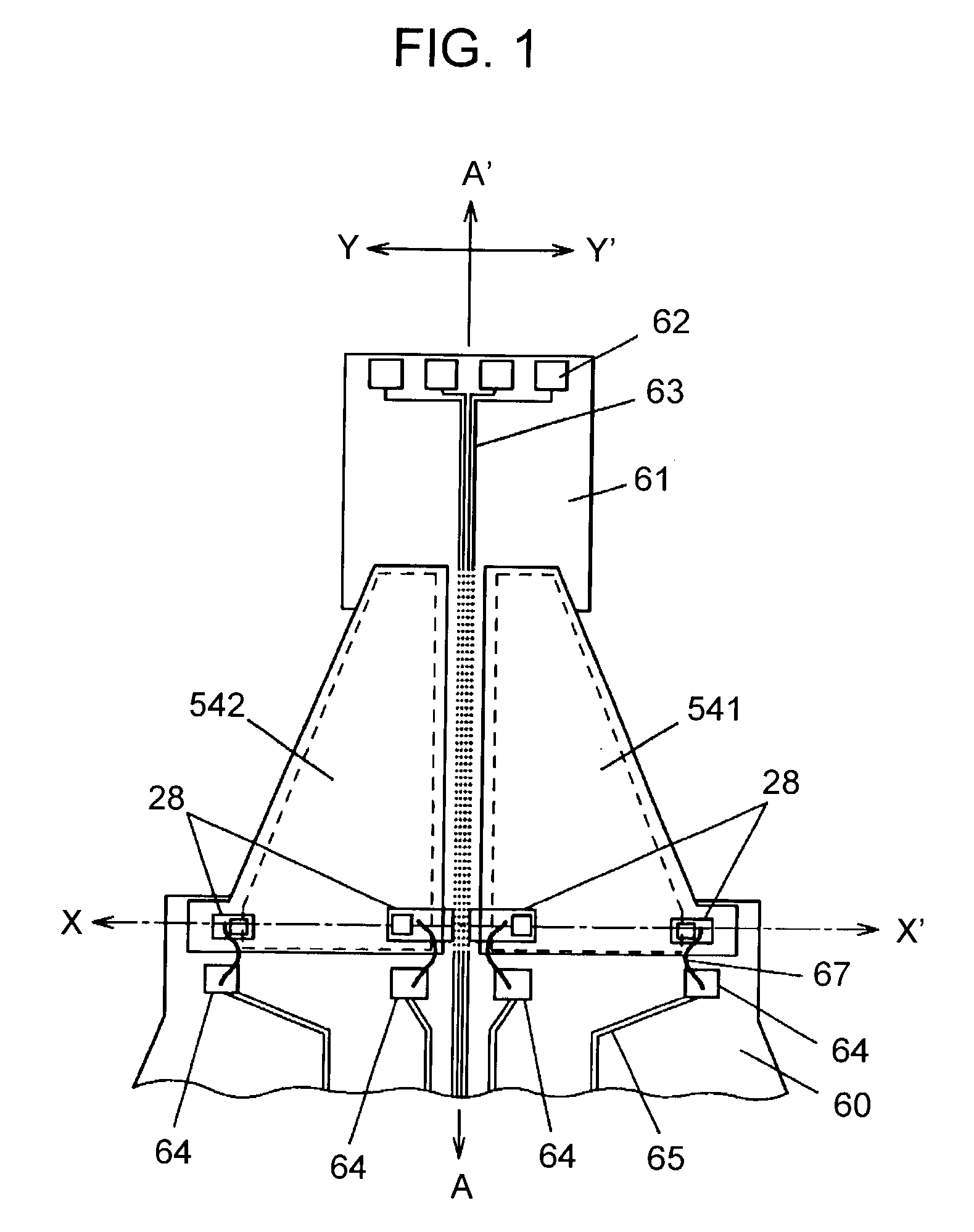
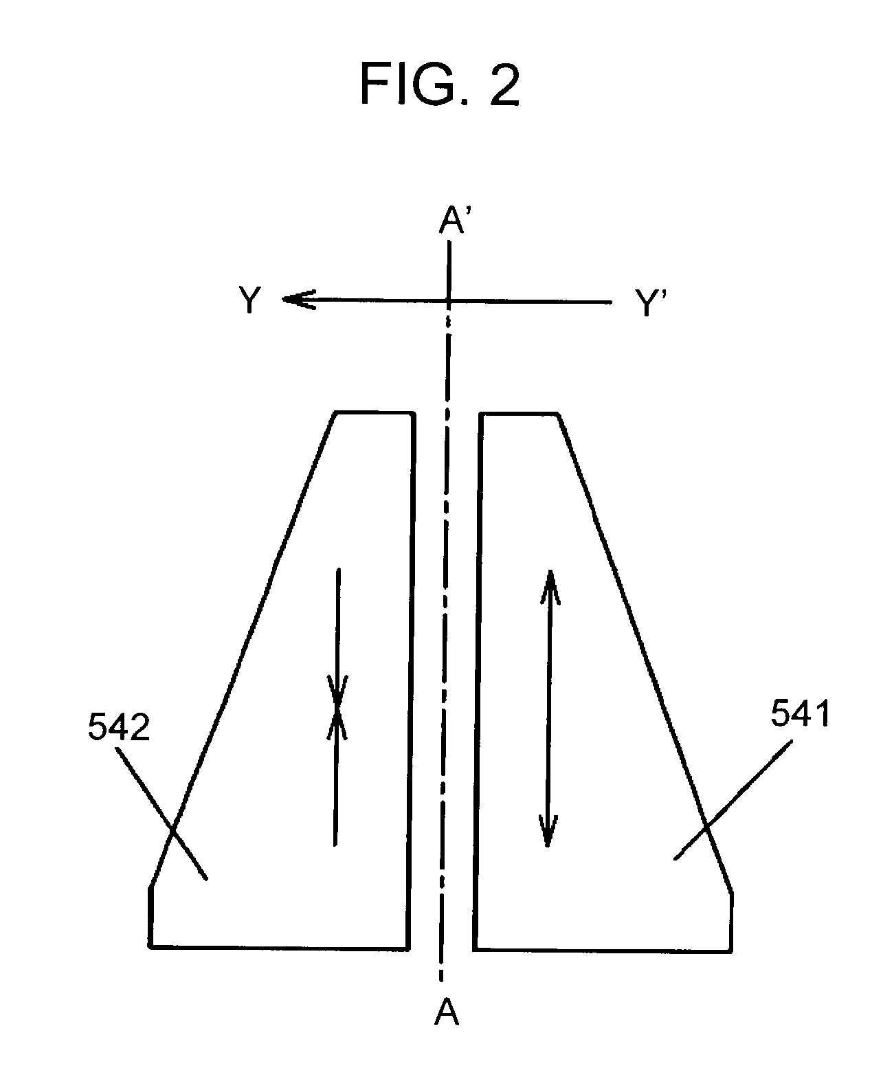
[0072]FIG. 1 shows a plan view of an actuator comprising thin film piezoelectric elements as a pair in a first exemplary embodiment of the present invention. The actuator is used for highly accurate fine positioning of a head slider to a predetermined track position on a disk in a magnetic recording and reproducing disk device. The actuator shown in FIG. 1 has two thin piezoelectric elements 541, 542. These thin film piezoelectric elements 541, 542 as a pair are structurally in a mirror-image relationship relative to each other against the A–A′ line, and are bonded to flexure 60 by an adhesive resin layer (not illustrated). After bonding, connection electrode pads 28 disposed on thin film piezoelectric elements 541, 542 are connected to piezoelectric electrode pad 64 disposed on flexure 60 by using, for example, wire leads 67, thereby forming an actuator for finely positioning a magnetic head.

[0073]Flexure 60 includes a slider holding portion 61 for fixing a head slider (not illustr...

second exemplary embodiment

[0114]Main steps for description of a manufacturing method of a second exemplary embodiment will be described with reference to FIG. 9A to FIG. 12B. Also in the second exemplary embodiment, an actuator with a pair of thin film piezoelectric elements as shown in FIG. 1 and FIG. 2 is explained as an example. Elements corresponding to those in FIG. 1 to FIG. 8B are given same reference numerals, and as for materials and processes, the same ones can be employed as with the first exemplary embodiment. In FIG. 9A to FIG. 9D and FIG. 10A to FIG. 10D, steps of processing on first substrate 81 and second substrate 91 are respectively shown. Steps of processing, after affixing these two substrates to each other, are shown in FIG. 11A to FIG. 11B and FIG. 12A to FIG. 12B.

[0115]First main electrode layer 82 is formed on first substrate 81, and after etching into a predetermined shape, first piezoelectric thin film 83 is formed on substrate 81 and electrode layer 82. An overall shape of first ma...

third exemplary embodiment

[0129]Main steps for description of a manufacturing method of a third exemplary embodiment of the present invention are shown in FIG. 13A to FIG. 14C. Also in the third exemplary embodiment, an actuator with paired thin film piezoelectric elements as shown in FIG. 1 and FIG. 2 is described as an example. Elements corresponding to those in FIG. 1 to FIG. 10D are given same reference numerals.

[0130]The manufacturing method of the present exemplary embodiment is different from that of the first exemplary embodiment with respect to material and configuration, a bonding method for piezoelectric thin films, and a method of forming an insulating resin layer. Steps different from those of the first exemplary embodiment are mainly explained in the following.

[0131]In FIG. 13A, first main electrode layer 2, first piezoelectric thin film 3, and first opposed electrode layer 105 are formed on first substrate 1, which electrode layers and thin film are formed into predetermined shapes. Also, as s...


PUM


Abstract

An actuator comprises first and second structures each with a piezoelectric layer sandwiched between a main electrode layer and an opposed electrode layer, which structures are formed on two substrates, respectively. A first main electrode layer and a first opposed electrode layer are provided with layer two projections, and a second opposed electrode layer is provided with one layer projection. Connection wiring is arranged for establishing connection, with the above two structures bonded to each other, between the layer projection of the first main electrode layer and the second main electrode layer, and between the layer projection of the first opposed electrode layer and the layer projection of the second opposed electrode layer. Thus, it is possible to provide an actuator which may assure highly accurate position control.

Description

FIELD OF THE INVENTION[0001]The present invention relates to a thin film piezoelectric element and its manufacturing method, and an actuator using the thin film piezoelectric element.BACKGROUND OF THE INVENTION[0002]With the recent advance of semiconductor technology, efforts are made in various ways to realize a micro-machine capable of considerable miniaturization with use of advanced semiconductor manufacturing technology, and electro-mechanical elements such as micro-actuators are now spotlighted. By using such elements, small-sized highly accurate mechanical components can be obtained, and productivity can be greatly improved by performing a semiconductor process. Particularly, micro-actuators using piezoelectric elements are used for fine displacement of a scanning tunneling microscope and for fine positioning of a head slider of a magnetic recording and reproducing disk device.[0003]For example, in a magnetic recording and reproducing disk device, a magnetic head for recordin...

Claims


Application Information

Patent Timeline
IPC IPC(8): G11B5/596H01L41/047H02N2/04G11B21/02G11B5/55G11B21/10H01L41/09H01L41/18H01L41/22H01L41/23H01L41/29H01L41/313
CPCH01L41/332H01L41/0986G11B5/596G11B21/10G11B5/5552H01L41/1876G11B5/484G11B5/4853G11B5/4873H10N30/206H10N30/8554H10N30/082
Inventor UCHIYAMA, HIROKAZU
Owner TDK CORPARATION
Why Eureka
Try Eureka