Method and apparatus for characterizing the propagation of noise through a cell in an integrated circuit

Active Publication Date: 2006-02-28
SYNOPSYS INC
View PDF33 Cites 12 Cited by
  • Summary
  • Abstract
  • Description
  • Claims
  • Application Information

AI Technical Summary

Benefits of technology

[0036]Drivers 102 and 104 and cell 110 can generally be any type of cell within an integrated circuit, such as a logic gate or a memory element. One advantage of the invention is that noise is calculated at the “cell level” using lookup tables, wherein a cell is comprised of a number of lower-level circuit elements, such as transistors. This saves a considerable amount of time over having to perform numerical simulations on larger numbers of lower-level circuit elements.
[0037]FIG. 2A illustrates an exemplary noise glitch in accordance with an embodiment of the invention. As is illustrated in FIG. 2, this exemplary noise glitch has an associated glitch height 201 and a glitch width 202.
[0038]FIG. 2B illustrates a noise immunity curve 204 in accordance with an embodiment of the invention. Note that this immunity curve is associated with a specific cell and a specific output load on the cell. For a given glitch width, noise immunity curve 204 indicates a minimum glitch height that causes a failure in the given cell. Glitches that fall above noise immunity curve 204 in noise failure region 210 generate failures, whereas glitches that fall below noise immunity curve 204 do not cause failures.Noise Glitches
[0039]As is illustrated in FIG. 3A, a coupling glitch 310 can be approximated by an idealized triangular glitch 320. Note that coupling glitch 310 and idealized triangular glitch 320 have the same maximum amplitudes, and that both curves exceed DC noise margin 325. Hence, each curve will cause a corresponding propagated glitch at the cell output as is illustrated in FIG. 3B.
[0040]In FIG. 3B, note that the propagated coupling glitch 330 has a greater magnitude that propagated triangular glitch 340. This is because the energy (or effective area) above the DC noise margin for coupling glitch 310 is larger than for idealized triangular glitch 320.Triangular Glitch Model
[0041]In order to remedy this problem, idealized triangular glitch 320 can be “smoothed” by feeding idealized triangular glitch 320 through an RC filter (as is illustrated in FIG. 4) to produce a smoothed triangular glitch 404. Note that the process of modeling propagation of a signal through an RC filter can be performed using well-known techniques without an unacceptable computational burden.

Problems solved by technology

Both of these factors are increasing the significance of noise caused by capacitive coupling between adjacent signal lines, and by inductive effects on long signal lines.
The above-described factors can cause “noise glitches” to be induced in signals lines within integrated circuits.
These noise glitches can cause timing degradation in switching nodes, or can cause false transitions in steady-state “quiet” nodes.
These false transitions can propagate through the circuit, and can cause functional errors or failures.
Otherwise, a chip may not function properly, and it may be necessary to perform a “mask re-spin,” which can cost hundreds of thousands (or possibly millions) of dollars and can significantly delay the release of a product.
Unfortunately, these timing simulations are presently unable to accurately simulate “noise glitches” over a large number of circuit elements.
However, such general-purpose circuit simulators are computationally intensive, and consequently require a significant amount of time to model noise on a small number of circuit elements.
This makes it impractical to simulate the effects of noise on larger circuits.

Method used


Image

  • Method and apparatus for characterizing the propagation of noise through a cell in an integrated circuit
  • Method and apparatus for characterizing the propagation of noise through a cell in an integrated circuit
  • Method and apparatus for characterizing the propagation of noise through a cell in an integrated circuit

Examples


Embodiment Construction
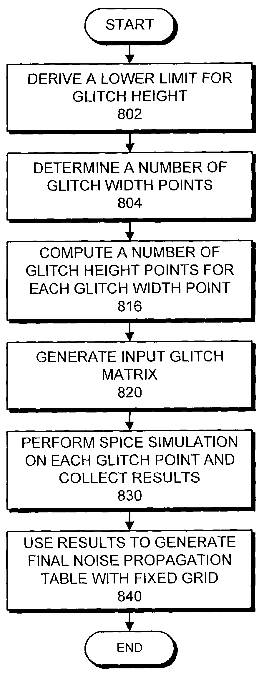
Modeling Noise

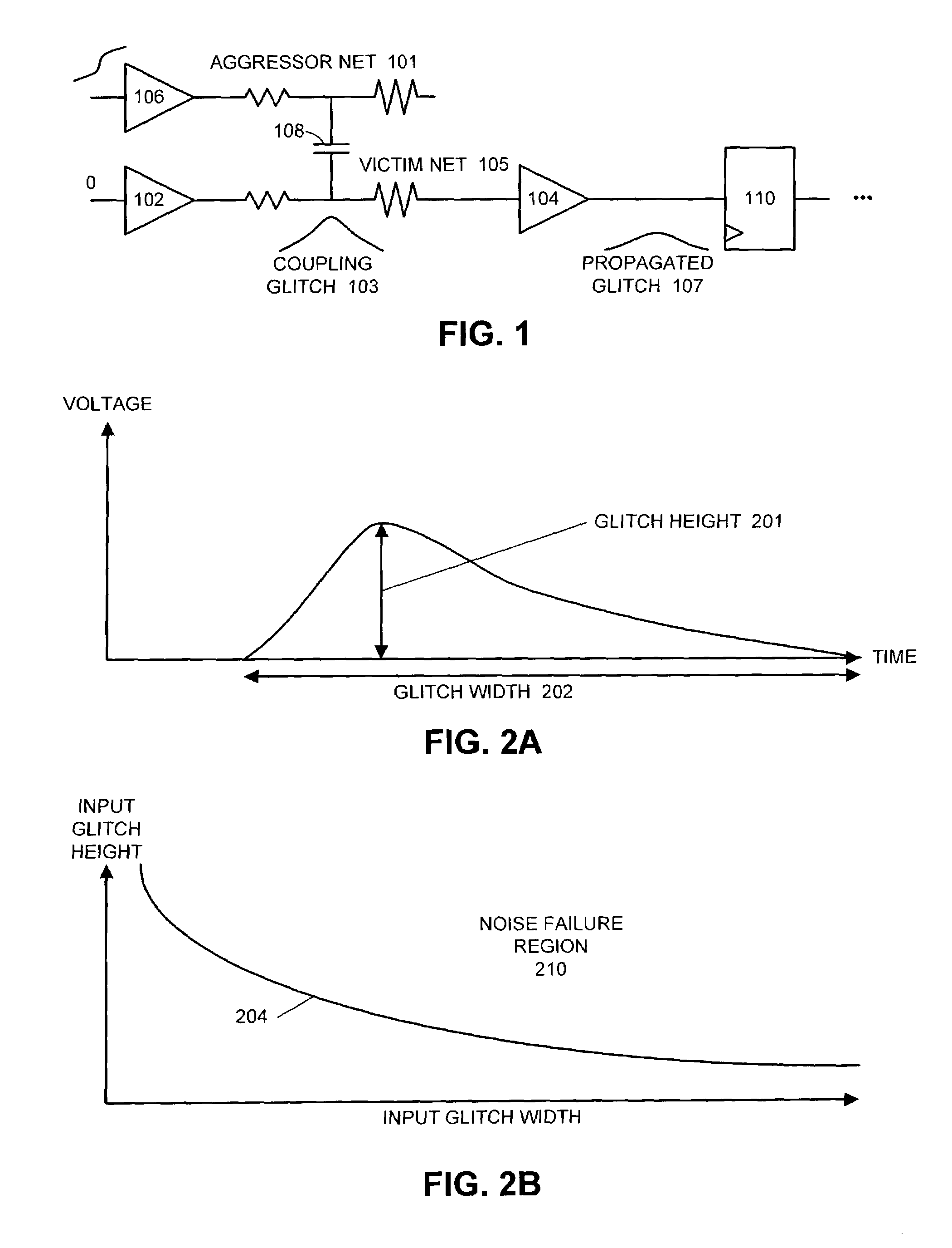
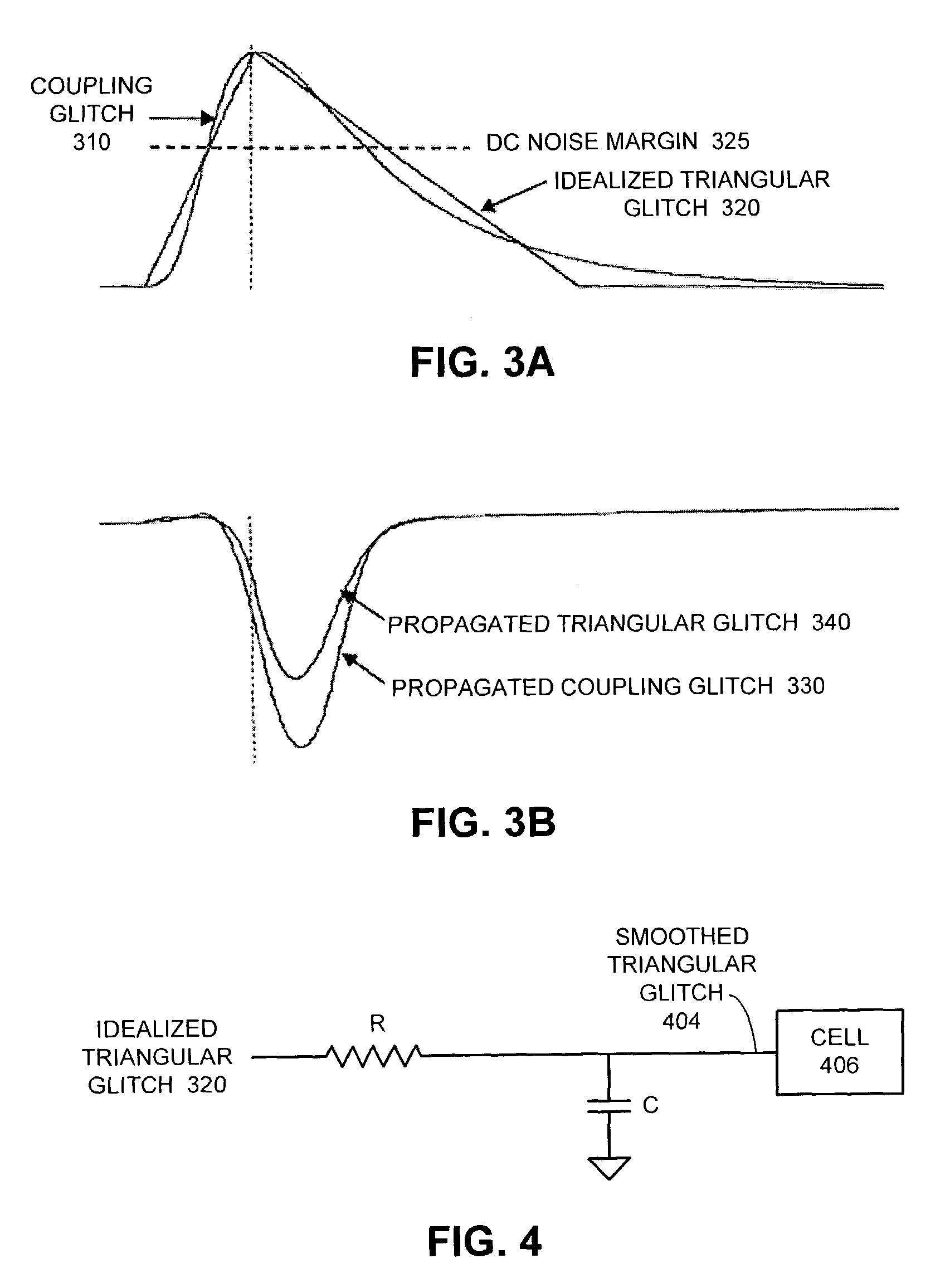
[0034]FIG. 1 illustrates how noise can be modeled in accordance with an embodiment of the invention. As is illustrated in FIG. 1, there is capacitive (and possibly inductive) coupling 108 between an aggressor net 101 and a neighboring victim net 105. Because of this coupling, a transition on aggressor net 101 induces a “coupling glitch”103 on victim net 105. Note that the I / V characteristics of an upstream driver 102, as well as the load on victim net 105 affect the size and shape of this coupling glitch 103.

[0035]Coupling glitch 103 feeds into a driver 104. If coupling glitch 103 has sufficient energy, it can cause a propagated glitch 107 at the output of driver 104. This propagated glitch 107 can possibly cause a functional failure in a downstream cell 110. Note that coupling glitch 103 can also combine with a propagated glitch from upstream driver 102 to generate an input noise signal for driver 104.

[0036]Drivers 102 and 104 and cell 110 can generally be any type of...


PUM


Abstract

One embodiment of the invention provides a system that characterizes cells within an integrated circuit. During operation, the system obtains a number of input noise signals to be applied to the cell. The system then simulates responses of the cell to each of the input noise signals, and stores a representation of the responses. This allows a subsequent analysis operation to access the stored representation to determine a response of the cell instead of having to perform a time-consuming simulation operation.

Description

RELATED APPLICATION[0001]The subject matter of this application is related to the subject matter in a co-pending non-provisional application by the same inventors as the instant application and filed on the same day as the instant application entitled, “Method and Apparatus for Detecting and Analyzing the Propagation of Noise Through an Integrated Circuit,” having Ser. No. 10 / 410,919, and filing date 9 Apr. 2003.BACKGROUND[0002]1. Field of the Invention[0003]The invention relates to techniques for modeling the performance of electrical circuits. More specifically, the invention relates to a method and an apparatus that uses a cell-level model to characterize and analyze the propagation of noise through an integrated circuit.[0004]2. Related Art[0005]Advances in semiconductor fabrication technology continue to decrease the minimum feature size that is attainable on an integrated circuit. This allows larger amounts of circuitry to be incorporated onto a single semiconductor die. At th...

Claims


Application Information

Patent Timeline
IPC IPC(8): G06F17/50G01R27/28G01R29/00G01R31/28G06F19/00
CPCG06F17/5036G06F30/367
Inventor GYURE, ALEXANDERZEJDA, JINDRICHFALLAH-TEHRANI, PEIVANDWANG, WENYUANLO, CHI-CHONGSHAHRAM, MAHMOUDLUO, YANSHENGSHU, WILLIAM CHIU-TINGKASNAVI, SEYED ALIREZA
Owner SYNOPSYS INC
Why Eureka
Try Eureka