

Heterojunction field effect transistor
a heterojunction field and transistor technology, applied in the field of semiconductor devices, can solve the problems of heterojunction field effect transistor series resistance increase, heterojunction field effect transistor voltage durability degradation, etc., and achieve the effect of small series resistance and high voltage durability
- Summary
- Abstract
- Description
- Claims
- Application Information
AI Technical Summary
Benefits of technology
Problems solved by technology
Method used
Image

Examples
first embodiment
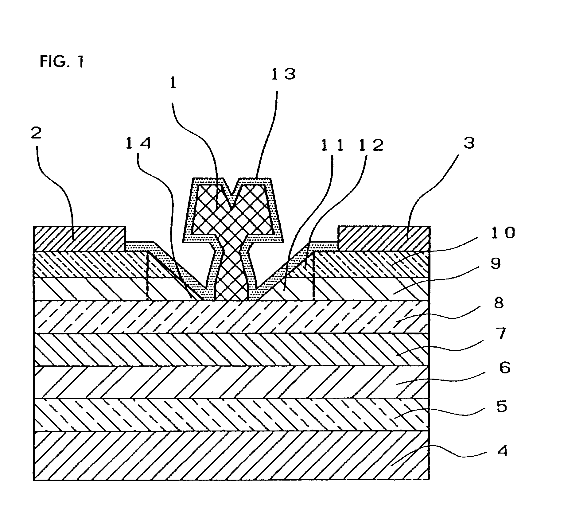
[0028][First Embodiment, FIG. 1]
[0029]In the following, description will be given to explain a heterojunction field effect transistor formed according to a first embodiment of the present invention, with reference to FIG. 1.
[0030]As shown in FIG. 1, a heterojunction field effect transistor having a one-step recess structure includes successively in the following order a semi-insulating substrate 4, a buffer layer 5, a channel layer 6, a first barrier layer 7, a second barrier layer 8, a lower contact layer 9 and a contact layer 10. In practice, these layers are all formed by an epitaxial growing method involving an MBE process or an MOCVD process and the like. Further, formed on the upper surface of the contact layer 10 are a source electrode 2 and a drain electrode 3. Here, the contact layer 10 forms an ohmic junction with the source electrode 2 and the drain electrode 3. Moreover, the contact layer 10 and the lower contact layer 9 are selectively recess-etched in their portions lo...
third embodiment
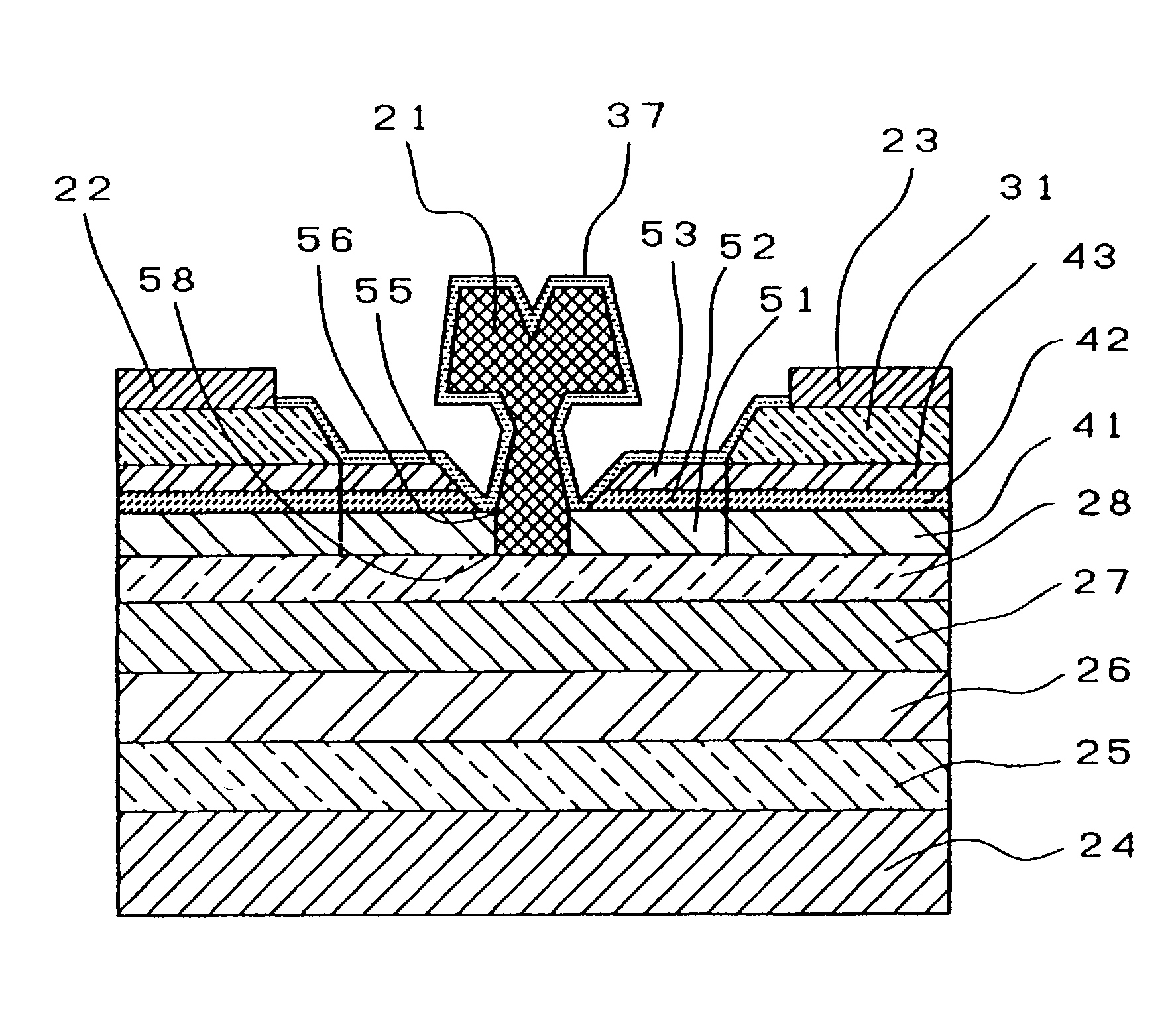
[0047][Third Embodiment, FIG. 4]
[0048]In the following, description will be given to explain a heterojunction field effect transistor formed according to a third embodiment of the present invention, with reference to FIG. 4.
[0049]As shown in FIG. 4, a heterojunction field effect transistor having a two-step recess structure is almost the same as the heterojunction field effect transistor formed according to the second embodiment, except that the eye-empty areas have a three-layer structure. Referring again to FIG. 4, the eye-empty areas include a first eye-empty area 51, a second eye-empty area 52 and a third eye-empty area 53. In detail, the first eye-empty area 51 is formed by part of a first connection layer 41 consisting of n-type AlGaAs having a low concentration which is for example 5×10¹⁷ to 2×1018 cm−3, the second eye-empty area 52 is formed by part of a second connection layer 42 consisting of n-type GaAs having a high concentration which is for example 2×10¹⁸ to 5×1018 cm−...
fifth embodiment
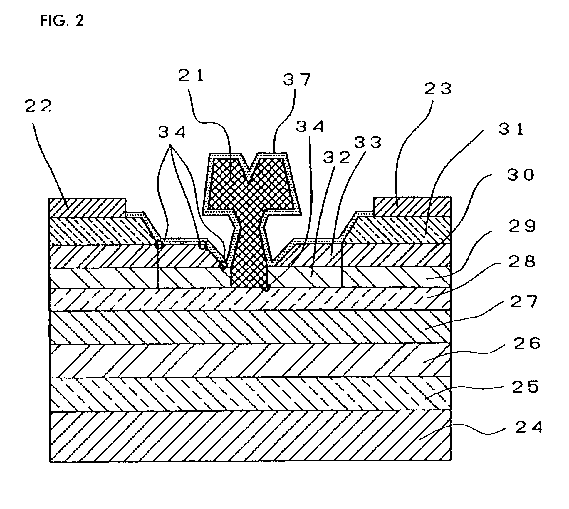
[0056][Fifth Embodiment, FIG. 6]
[0057]In the following, description will be given to explain a heterojunction field effect transistor formed according to a fifth embodiment of the present invention, with reference to FIG. 6.
[0058]As shown in FIG. 6, a heterojunction field effect transistor of the fifth embodiment is almost the same as the heterojunction field effect transistor formed according to the fourth embodiment, except that the eye-empty areas have a six-layer structure. Referring again to FIG. 6, the eye-empty areas include a first eye-empty area 91, a second eye-empty area 92, a third eye-empty area 93, a fourth eye-empty area 94, a fifth eye-empty area 95 and a sixth eye-empty area 96. In detail, the first eye-empty area 91 is formed by part of a first connection layer 81 consisting of a low concentration n-type AlGaAs, the second eye-empty area 92 is formed by part of a second connection layer 82 consisting of n-type AlGaAs, the third eye-empty layer 93 is formed by part ...
PUM
 Abstract
Description
Claims
Application Information