Thin film transistor and method of fabricating the same

Inactive Publication Date: 2006-03-21
CANON KK
View PDF32 Cites 31 Cited by
  • Summary
  • Abstract
  • Description
  • Claims
  • Application Information

AI Technical Summary

Benefits of technology

[0014]In the present invention, the use of zirconium oxide or hafnium oxide as a gate insulating film makes it possible to reduce the interface state density between an active layer made of non-single-crystal germaniu

Problems solved by technology

However, no non-single-crystal germanium TFT has been put into practical use.
Note also

Method used


Image

  • Thin film transistor and method of fabricating the same
  • Thin film transistor and method of fabricating the same
  • Thin film transistor and method of fabricating the same

Examples


first embodiment

[First Embodiment]

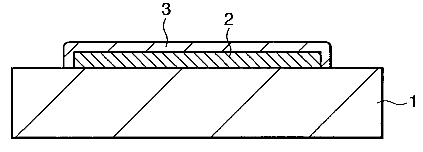
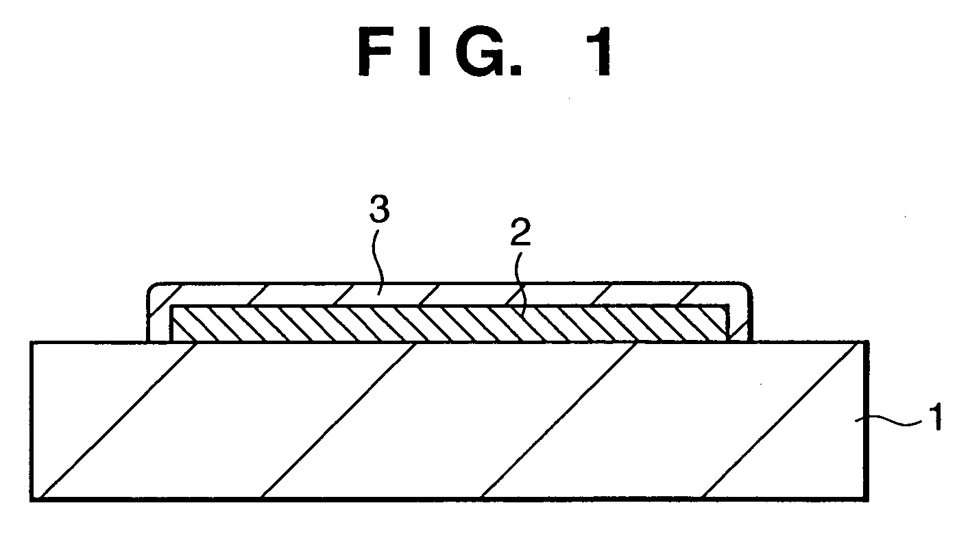
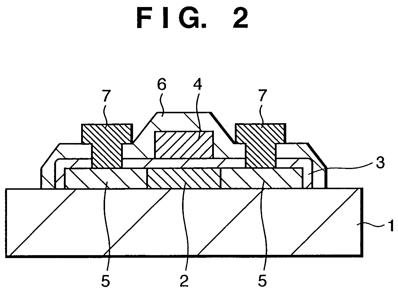
[0022]A thin film transistor and a method of fabricating the same according to the first embodiment of the present invention will be described below with reference to FIGS. 1 and 2.

[0023]As shown in FIG. 1, a non-single-crystal germanium film 2 is formed on a substrate 1 to form a TFT active layer. On the non-single-crystal germanium film 2, an oxide film 3 substantially made of zirconium oxide or hafnium oxide is formed to form a gate oxide film.

[0024]As shown in FIG. 2, a gate electrode 4 is formed on the oxide film 3 to form a planar TFT having the non-single-crystal germanium active layer 2 and the gate oxide film 3 substantially made of zirconium oxide or hafnium oxide. Reference numerals 5 denote source and drain regions defined in the active layer 2; 6, a protective film; and 7, source and drain electrodes.

second embodiment

[Second Embodiment]

[0025]A thin film transistor and a method of fabricating the same according to the second embodiment of the present invention will be described below with reference to FIGS. 3 and 4.

[0026]As shown in FIG. 3, a gate electrode 4 is formed on a substrate 1, and an oxide film 3 substantially made of zirconium oxide or hafnium oxide is formed on the gate electrode 4. Then, an active layer 2 made of a non-single-crystal germanium film is formed.

[0027]As shown in FIG. 4, source and drain regions 5 are formed in the active layer 2 to form a staggered TFT having the non-single-crystal germanium active layer 2 and the gate oxide film 3 substantially made of zirconium oxide or hafnium oxide. Reference numerals 7 denote source and drain electrodes.

[0028]Examples of a substrate preferably usable in the present invention are glass and polyimide.

[0029]Also, examples of non-single-crystal germanium preferably usable in the present invention are amorphous germanium, polycrystallin...


PUM


Abstract

Provided is a non-single-crystal germanium thin film transistor having a gate insulating film capable of reducing the interface state density between an active layer and the gate insulating film. This thin film transistor has an active layer made of a non-single-crystal germanium film, and a gate oxide film substantially made of zirconium oxide or hafnium oxide.

Description

FIELD OF THE INVENTION[0001]The present invention relates to a TFT (Thin Film Transistor) having a non-single-crystal germanium film as an active layer, and a method of fabricating the same.BACKGROUND OF THE INVENTION[0002]A thin film transistor having a non-single-crystal germanium film as an active layer (this transistor will be referred to as a non-single-crystal germanium TFT hereinafter) has high mobility and high drivability, and is superior in these characteristics to a thin film transistor having a non-single-crystal silicon film as an active layer (this transistor will be referred to as a non-single-crystal silicon TFT hereinafter). Also, the non-single-crystal germanium TFT can be fabricated at a lower temperature than that for the non-single-crystal silicon TFT. Therefore, it is expected to widen the range of selection of substrates, and realize larger areas and more flexible substrates. For example, thin film transistors having a non-single-crystal germanium film as an a...

Claims


Application Information

Patent Timeline
IPC IPC(8): H01L29/04H01L21/336H01L29/49H01L29/786
CPCH01L29/4908H01L29/78684H01L29/66742
Inventor YONEHARA, TAKAOSHIMADA, TETSUYA
Owner CANON KK
Why Eureka
Try Eureka