Method of producing a composite sheet and method of producing a laminate by using the composite sheet

Inactive Publication Date: 2006-03-28
KYOCERA CORP
View PDF16 Cites 6 Cited by
  • Summary
  • Abstract
  • Description
  • Claims
  • Application Information

AI Technical Summary

Benefits of technology

[0031]It is therefore an object of the present invention to provide a method of producing a composite sheet in which another material is uniformly buried in a portion of a first ce

Problems solved by technology

As for the electrical characteristics, further, a delay in the signals causes a problem as the operation speed increases, and it has been desired to use a wiring conductor having a small wiring conductor loss, i.e., to use a wiring conductor having a low resistance.
In the wiring conductor in which the wirings are densely arranged, however, the wire width of the wiring pattern is limited by the area of the multi-layer wiring board and cannot be increased beyond a predetermined width.
Besides, with the above method of forming the wiring conductor, it is difficult to obtain a wiring conductor having a sufficient thickness at a low cost within short periods of time without adversely affecting the subsequent steps.
Therefore, the above requirement of decreasing the resistance is not satisfied.
At this moment, the surfaces of the portions filled with the paste become rugged such as dented.
When a green sheet is laminated, therefore, the laminate becom

Method used


Image

  • Method of producing a composite sheet and method of producing a laminate by using the composite sheet
  • Method of producing a composite sheet and method of producing a laminate by using the composite sheet
  • Method of producing a composite sheet and method of producing a laminate by using the composite sheet

Examples


example 1

(Preparation of a First Ceramic Sheet)

[0286]To 100 parts by mass of a ceramic composition comprising 60% by volume of a glass powder having an average particle size of 1.8 μm and 40% by volume of an alumina powder having an average particle size of 2.4 μm, there were added 12 parts by mass of a polyisobutyl methacrylate as an organic binder and 54 parts by mass of toluene as a solvent. The mixture was mixed together with a ball mill for 24 hours to prepare a slurry thereof.

[0287]By using this slurry, a first ceramic sheet A measuring 20 mm long, 20 mm wide and 120 μm thick was prepared by the doctor blade method.

[0288]A metal paste was prepared by mixing 100 parts by mass of a copper powder having an average particle size of 1.5 μm, 12 parts by mass of an acrylic resin as an organic binder and 10 parts by mass of terpineol as a solvent, and was applied onto the surface of the first ceramic green sheet A in a predetermined pattern by the screen-printing method.

[0289]Further, through ...

example 2

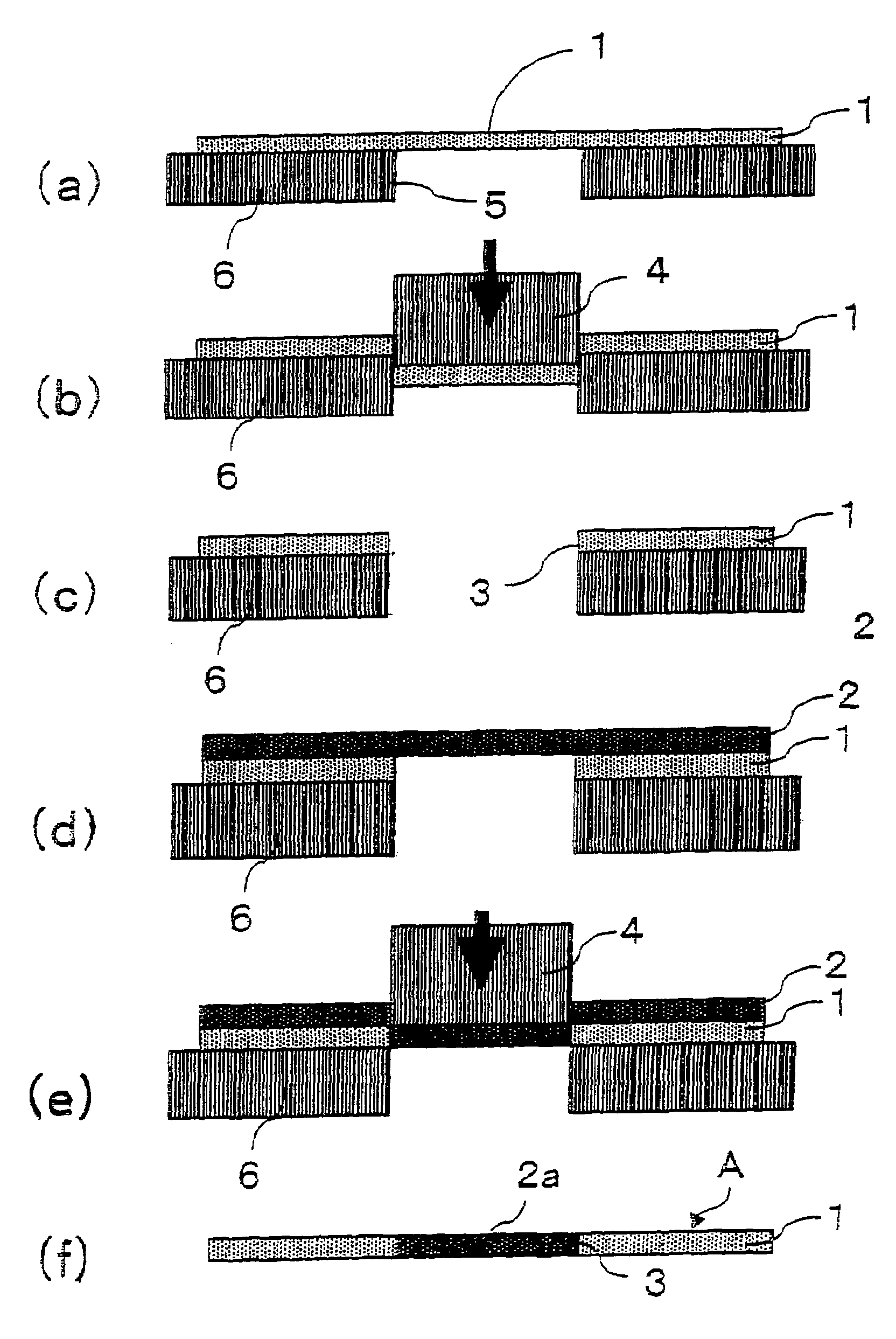
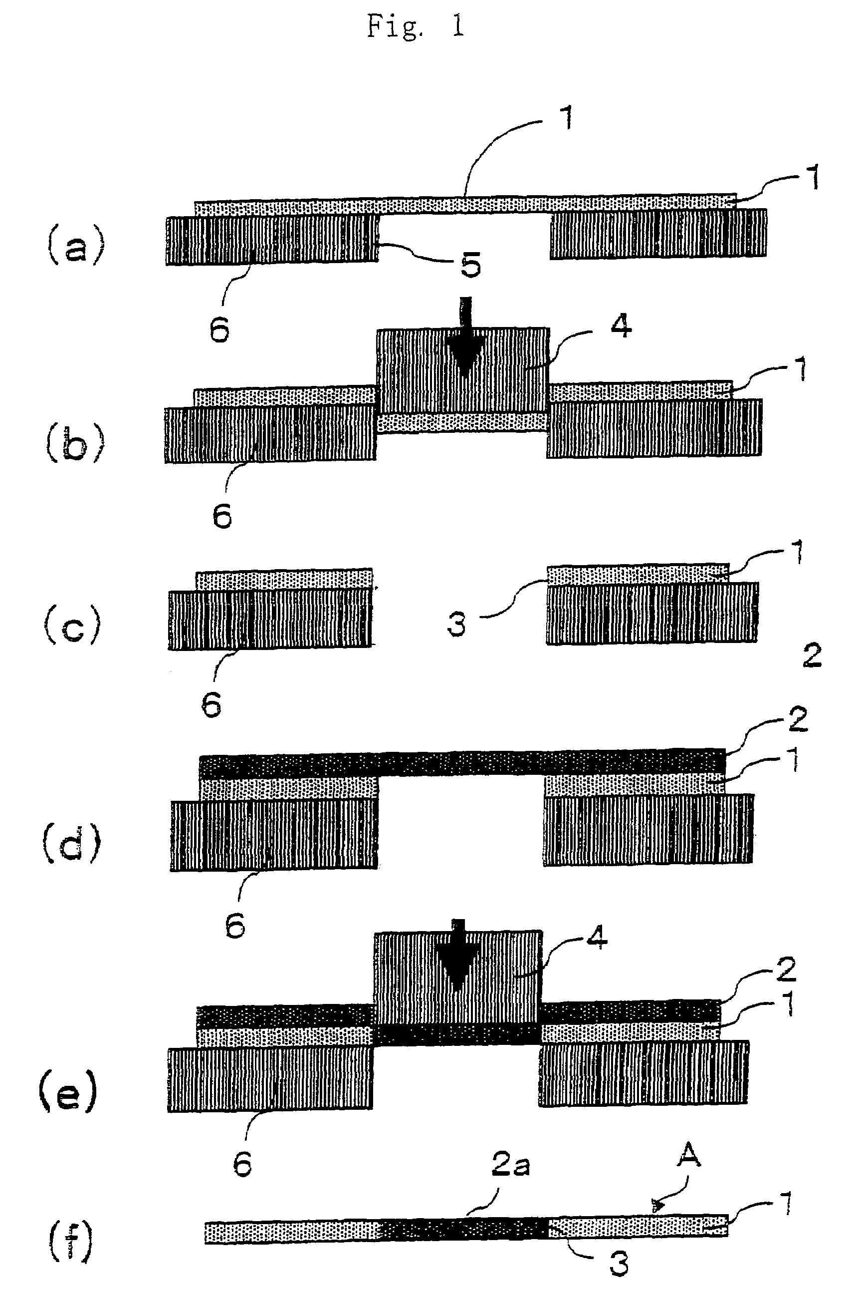
[0301]The first ceramic sheet A and the resin sheet B prepared in Example 1 were laminated as shown in FIG. 2. Then, the upper punch of the punching device was lowered until the lower surface of the upper punch was in flush with the surface of the sheet A.

[0302]The upper punch was raised, and it was confirmed that there had been formed a composite sheet C3 of a structure with the resin sheet B being buried in the through hole of the first ceramic sheet A.

[0303]Next, a total of five layers of green sheets were laminated in quite the same manner as in Example 1 by using an adhering solution, i.e., the composite sheet C3, a composite sheet C4 prepared in the same manner as C3, and ceramic green sheets D1, D2 and D3 on which an ordinary wiring pattern has formed but which have not been compounded, and the laminate was heated at a temperature of 60° C. under a pressure of 5 MPa.

[0304]The thus press-laminated sample was observed for its deformation of the ceramic green sheet at the portio...

example 3

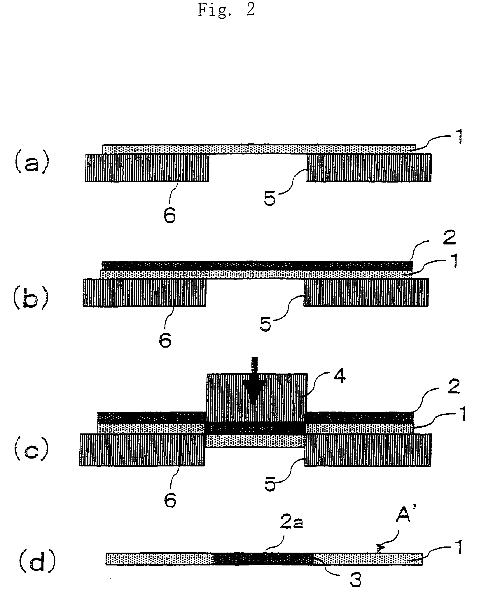
[0316]To 100 parts by mass of a ceramic composition comprising 60% by mass of a carbon powder having an average particle diameter of 40 μm and 40% by mass of a butyral resin having a glass transition point of 60° C., there was added 150 parts by mass of toluene and then the components were mixed.

[0317]Then, the mixture was stirred with a ball mill to prepare a slurry.

[0318]The slurry was deformed by stirring under reduced pressure, and then using the deformed slurry, there was formed a burn-and-extinguish sheer having 200 μm thickness by doctor-blade method.

[0319]A ceramic wiring substrate having a cavity was prepared quite the same manner as Example 1 except that the above mentioned carbon sheet was used instead of a resin sheet as a burn-and-extinguish sheet.

[0320]In the preparation steps, the press-laminated sample was observed for its deformation of the ceramic green sheet at the portion where the burn-and-extinguish sheet (carbon sheet) was buried.

[0321]However, no deformation ...


PUM

PropertyMeasurementUnit
Percent by volumeaaaaaaaaaa
Particle sizeaaaaaaaaaa

Abstract

A method of producing a composite sheet in which a through hole formed in a predetermined portion of the first ceramic sheet is buried with a different kind of sheet having substantially the same thickness as the first ceramic sheet, such as a resin sheet a metal sheet or a ceramic sheet of a material different from that of the first ceramic sheet. A first method comprises a step of preparing a first ceramic sheet from a ceramic powder, and a different kind of sheet; a step of forming a through hole in a predetermined portion of the first ceramic sheet; a step of laminating the different kind of sheet on the ceramic sheet in which the through hole is formed; and a step of preparing a composite sheet by pressing the portion of the first ceramic sheet where the through hole is formed from the side of the different kind of sheet, such that the first ceramic sheet and the different kind of sheet are integrated together. A second method comprises a step of preparing a first ceramic sheet and a different kind of sheet, and laminating the first ceramic sheet and the different kind of sheet one upon the other; and a step of preparing a composite sheet by pressing a predetermined portion of the laminate from the side of the different kind of sheet, such that the pressed portion of the different kind of sheet is transferred onto the side of the first ceramic sheet to integrate the first ceramic sheet and the different kind of sheet together. A further method is for producing a laminate by laminating the obtained composite sheet on other first ceramic sheet or on other composite sheet.

Description

BACKGROUND OF THE INVENTION[0001]1. Field of the Invention[0002]The present invention relates to a method of producing a composite sheet including a ceramic layer and to a method of producing a laminate by using the composite sheet. More particularly, the invention relates to a method of producing a composite sheet that is preferably used for the production of a variety of wiring boards and a wiring board applied to packages for containing semiconductor devices, and is particularly used for the production of ceramic boards having wiring conductors capable of radiating the heat and permitting the flow of heavy currents of power module boards. The invention further relates to a method of producing a laminate such as a wiring board using the composite sheet.[0003]2. Description of the Related Art[0004]In recent years, the semiconductor devices are generating the heat in ever increased amounts accompanying the trend toward highly densely integrating the semiconductor devices.[0005]In or...

Claims


Application Information

Patent Timeline
IPC IPC(8): B28B3/00C04B35/111C04B35/195C04B35/20H01L21/48H01L23/498H05K1/03H05K3/00H05K3/40H05K3/46
CPCB32B18/00C04B35/111C04B35/195C04B35/20H01L21/481H05K3/0014H05K3/4061Y10T156/1057B32B2311/12B32B2315/02C04B2235/3206C04B2235/3217C04B2235/3267C04B2235/3418C04B2235/3445C04B2235/3481C04B2235/404C04B2235/6025C04B2235/608C04B2235/652C04B2237/341C04B2237/343C04B2237/40C04B2237/403C04B2237/407C04B2237/50C04B2237/62C04B2237/68C04B2237/704C04B2237/706H01L23/49894H05K1/0306H05K3/005H05K3/4611H05K3/4629H05K2203/033H05K2203/308H01L2924/0002B32B2309/022Y10T29/49163Y10T156/107Y10T156/1056H01L2924/00
Inventor SUZUKI, SHINICHINAGATA, KOICHIIKEUCHI, TAKAYUKITANAKA, YUJISASAKI, YASUHIROYAMADA, SHIGEKIYOSHIHARA, YASUHIKOONITANI, MASAMITSU
Owner KYOCERA CORP
Why Eureka
Try Eureka