Structure for interconnecting conductors and connecting method
- Summary
- Abstract
- Description
- Claims
- Application Information
AI Technical Summary
Benefits of technology
Problems solved by technology
Method used
Image

Examples
Embodiment Construction
[0031]Other features and advantages of the present invention will become clearer from the description given below with reference to the accompanying drawings.
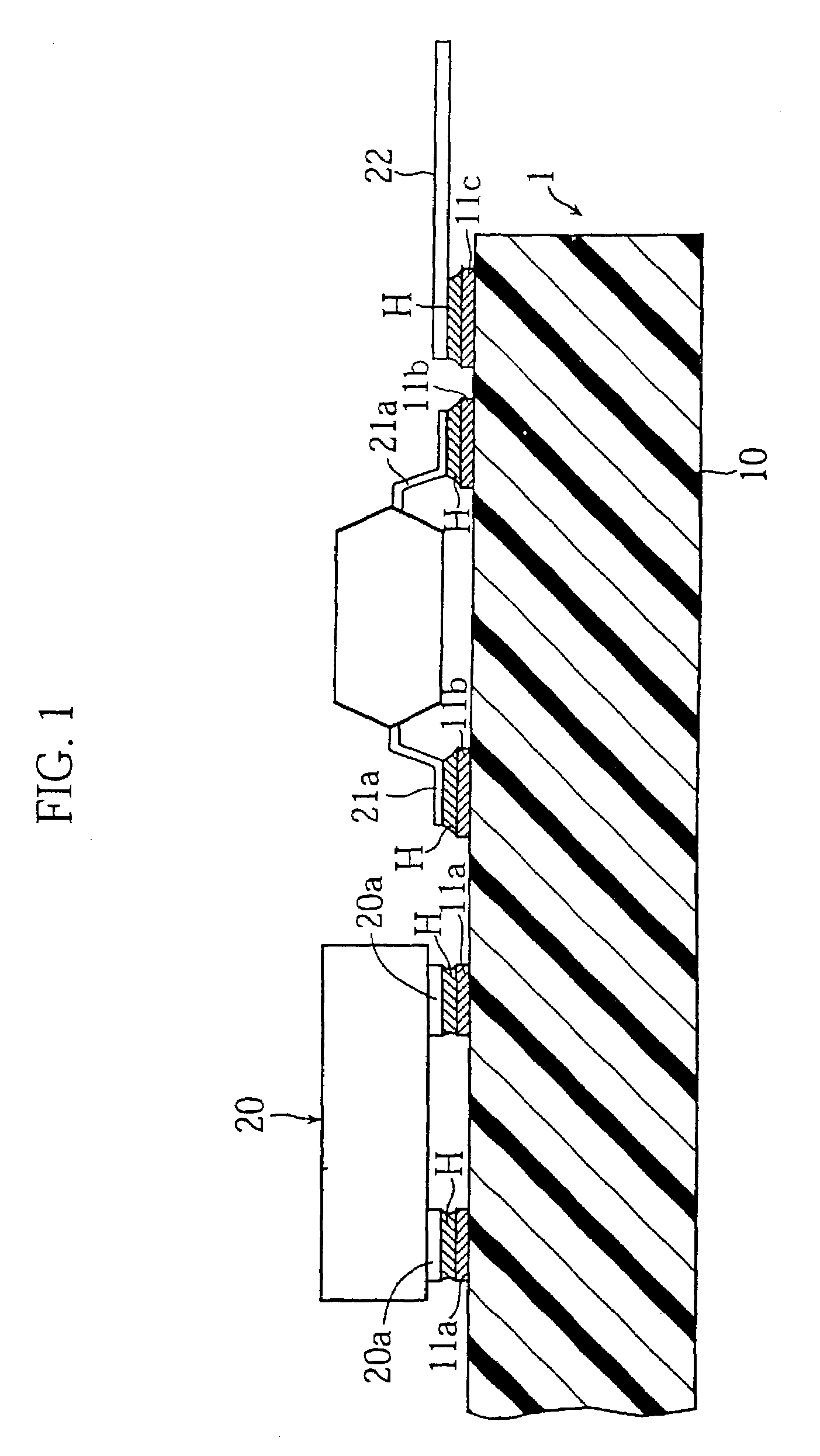
[0032]A preferred embodiment of the present invention will be described below in detail with reference to FIG. 1. FIG. 1 is a sectional view illustrating a connection structure of conductors according to an embodiment of the present invention.
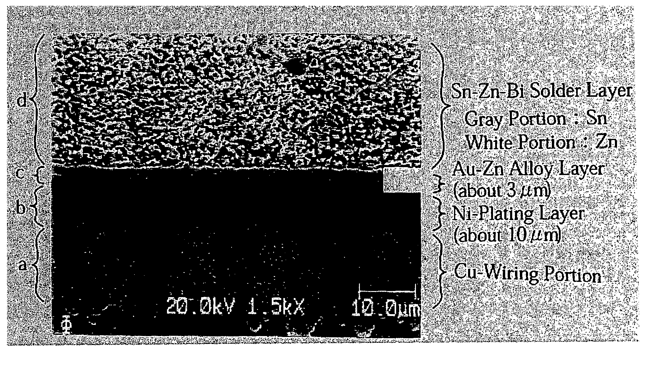
[0033]In FIG. 1, a circuit board 1 includes a protective circuit for preventing the overcharge of a rechargeable battery for example. The circuit board 1 comprises a substrate 10 formed of, for example, glass-fiber-reinforced epoxy resin, and a wiring pattern (not shown) of Cu formed on the substrate. The Cu wiring pattern may be provided by forming a Cu film having a thickness of about 15˜25 μm entirely on a surface of the substrate 10 by CVD or vapor deposition for example and then removing unnecessary portions by etching.
[0034]The Cu wiring pattern is provided, at appropriate portions t...
PUM
| Property | Measurement | Unit |
|---|---|---|
| Thickness | aaaaa | aaaaa |
| Composition | aaaaa | aaaaa |
| Structure | aaaaa | aaaaa |
Abstract
Description
Claims
Application Information