Broadband light emitting device

a light-emitting device and wide-band technology, applied in the direction of laser optical resonator construction, nanotechnology, lasers, etc., can solve the problems of difficult implementation, trivial control of quantum dot size dispersions, and difficulty in reproducing, so as to increase the quantum dot height and widen the emission spectrum

Active Publication Date: 2006-03-28
EXALOS
View PDF3 Cites 169 Cited by
  • Summary
  • Abstract
  • Description
  • Claims
  • Application Information

AI Technical Summary

Benefits of technology

[0014]Several reasons may be expected to contribute to the effect that the emission wavelength depends on the composition of the adjoining layer or adjoining layers. Firstly, the barrier height confining the quantum dot electronic states changes. Secondly, the strain induced on the quantum dot material by the adjoining layer depends on the adjoining layer's lattice constant which is dependent on the material composition. A third possible effect may arise depending on the material compositions of the quantum dots and of the adjoining layer: If the chemical elements making up the quantum dots are also present in the adjoining layer material, the quantum dots may grow further than they would from just the quantum dot layer deposited material. Material from the adjoining layer may thus “adhere” to the quantum dot. This may be because of activated spinoidal decomposition of the adjoining layer, which may in deposits preferentially be on the strained region on top of the QD and thus increase the quantum dot heights. Also, it is possible that the chemical composition of the quantum dot itself changes dependent on the adjoining layer's composition, due to diffusion effects. What is important is that the wavelength may be influenced based on parameters of the adjoining layer, which principle allows to stick to the optimal growth conditions when fabricating the quantum dot layer and to tune the emission spectrum in a separate step, namely in the adjoining layer fabrication step.
[0015]The invention uses this insight that the optical transition or the optical transitions can be engineered by varying the surrounding material, i.e. the material of the adjoining layer. Thereby, controlling the quantum dot emission wavelength—and ultimately the SLED emission spectrum—by varying the adjoining layer material is possible. By stacking quantum dot layers with different adjoining layer materials or adjoining layer thicknesses, a wide emission spectrum can be achieved.

Problems solved by technology

However, the exact control of the quantum dot size dispersions is neither trivial nor easily reproducible.
Since the amount of InAs also affects the density and radiative efficiency of the quantum dots (QDs), this last approach is difficult to implement, too.

Method used


Image

  • Broadband light emitting device
  • Broadband light emitting device
  • Broadband light emitting device

Examples


Embodiment Construction

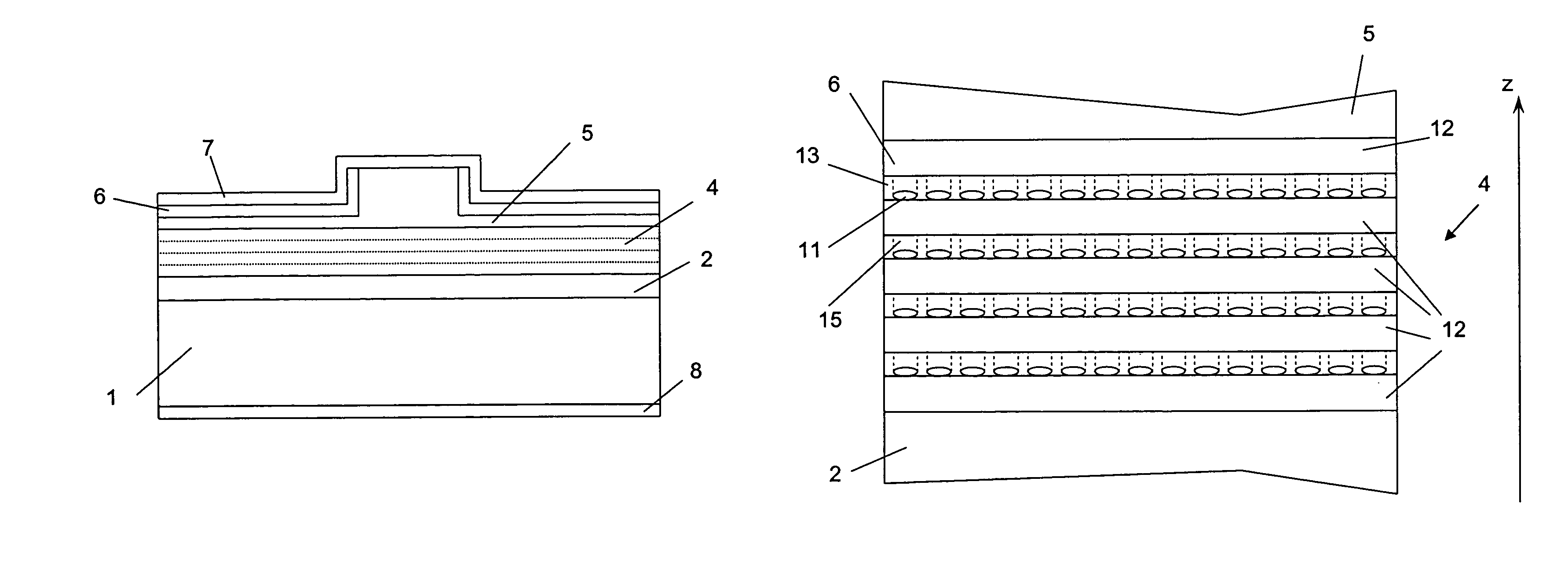
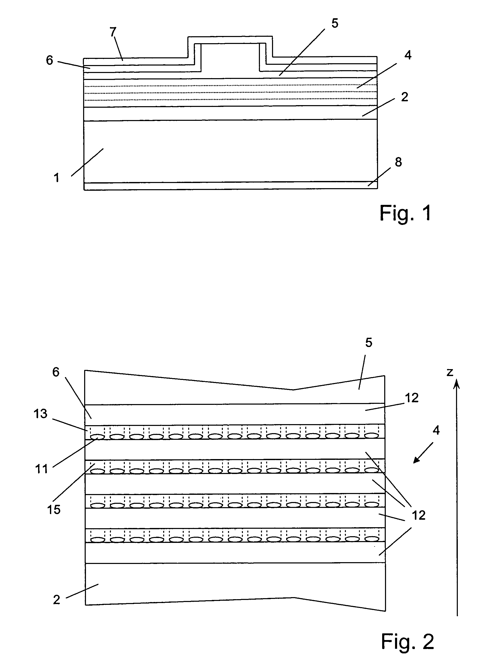
[0027]The device schematically shown in FIG. 1 is suitable for emission around a technologically important wavelength of 1.3 μm. It comprises a semiconductor heterostructure including a GaAs substrate 1. The substrate comprises an Si-doped (the Si doping here being an n-doping) InGaP or AlGaAs semiconductor cladding layer 2. On top of the Si-doped cladding layer, a layered structure 4 forming a PN-junction and comprising the active zone is placed. The layered structure 4 comprises a plurality of layers of quantum dots, as will be explained in more detail below. On the layered structure 4, there is a second cladding layer 5 with a ridge structure. The embodiment of the figure further comprises a thin insulating layer 6, for example an oxide layer, and a top electrode layer 7. A second electrode 8 (or bottom electrode) is provided on the backside of the substrate 1. Upon injection of a current—the current flows between the top and the bottom electrode—electroluminescence generates rad...


PUM


Abstract

The invention concerns a superluminescent light emitting diode (SLED) comprising a semiconductor heterostructure forming a PN junction and a waveguide. The semiconductor heterostructure includes a gain region with a contact means for biasing the PN junction so as to produce light emission including stimulated emission from an active zone of the gain region, and in the active zone a plurality of quantum dot layers, each quantum dot layer made up of a plurality of quantum dots and a plurality of adjoining layers, each adjoining layer adjacent to one of said quantum dot layers. The material composition or a deposition parameter of at least two adjoining layers is different. This ensures an enhanced emission spectral width.

Description

FIELD OF THE INVENTION[0001]This invention is in the field of broadband light emitting devices. It more particularly relates to superluminescent light emitting diodes (SLEDs), to Semiconductor Optical Amplifiers (SOAs), to External Cavity Semiconductor lasers and other broadband electroluminescent devices and to methods of producing superluminescent light emitting diodes.BACKGROUND OF THE INVENTION[0002]Superluminescent light emitting diodes (SLEDs) are diodes that, when biased in the forward direction, become optically active and generate amplified spontaneous emission over a wide range of wavelengths.[0003]SLEDs (sometimes also called Superluminescent diodes, SLDs) are attractive for applications in which a higher intensity than the one emitted by conventional LEDs is required, but where an even distribution of the emitted wavelength over a broad spectral range is desired. In a SLED for delivering a large incoherent light output from a first end facet, it is thus important to supp...

Claims


Application Information

Patent Timeline
Patent Type & Authority Patents(United States)
IPC IPC(8): H01L29/06H01L31/0328H01L31/0336H01L31/072H01L31/109H01L33/00H01L33/06H01L33/08H01S5/14H01S5/223H01S5/34H01S5/343
CPCB82Y10/00B82Y20/00H01L33/0045H01S5/14H01S5/2231H01L33/08H01L33/06H01S5/34353H01S5/3412H01S5/34313
Inventor LI, LIANHEFIORE, ANDREAOCCHI, LORENZOVELEZ, CHRISTIAN
Owner EXALOS
Why Eureka
Try Eureka