Method of crystallizing amorphous silicon layer and crystallizing apparatus thereof

a technology of crystallizing apparatus and amorphous silicon, which is applied in the direction of polycrystalline material growth, chemically reactive gas growth, crystal growth process, etc., can solve the problems of difficult forming polysilicon on a substrate having a wide area, high temperature and long crystallization processing time of solid phase crystallization, etc., to accelerate the crystallization of amorphous silicon, reduce the crystallization temperature, and alleviate metal contamination

Inactive Publication Date: 2006-04-04
JANG JIN
View PDF4 Cites 4 Cited by
  • Summary
  • Abstract
  • Description
  • Claims
  • Application Information

AI Technical Summary

Benefits of technology

[0017]The object of the present invention is to provide a method of crystallizing an amorphous silicon layer and a crystallizing apparatus thereof which accelerate the crystallization of amorphous silicon by use of plasma while decreasing crystallization temperature.
[0018]Another object of the present invention is to p

Problems solved by technology

When providing low temperature crystallization under 400° C., which is disclosed in Hiroyaki Kuriyama, et al., Jpn. J. Appl. Phys., 31, 4550 (1992), the laser crystallization fails to provide uniform crystallization and has difficulty in forming polysilicon on a substrate having a wide area due to an expensive apparatus and low productivity.
However, the solid phase crystallization requires high temperature and long crystallization processing time.
Such process is seldomly applied to forming polysilicon on a glass substrate and has low productivity.
Metal-induced crystallization has a crystallization temp

Method used


Image

  • Method of crystallizing amorphous silicon layer and crystallizing apparatus thereof
  • Method of crystallizing amorphous silicon layer and crystallizing apparatus thereof
  • Method of crystallizing amorphous silicon layer and crystallizing apparatus thereof

Examples


Embodiment Construction

[0038]Reference will now be made in detail to the preferred embodiments of the present invention, examples of which are illustrated in the accompanying drawings.

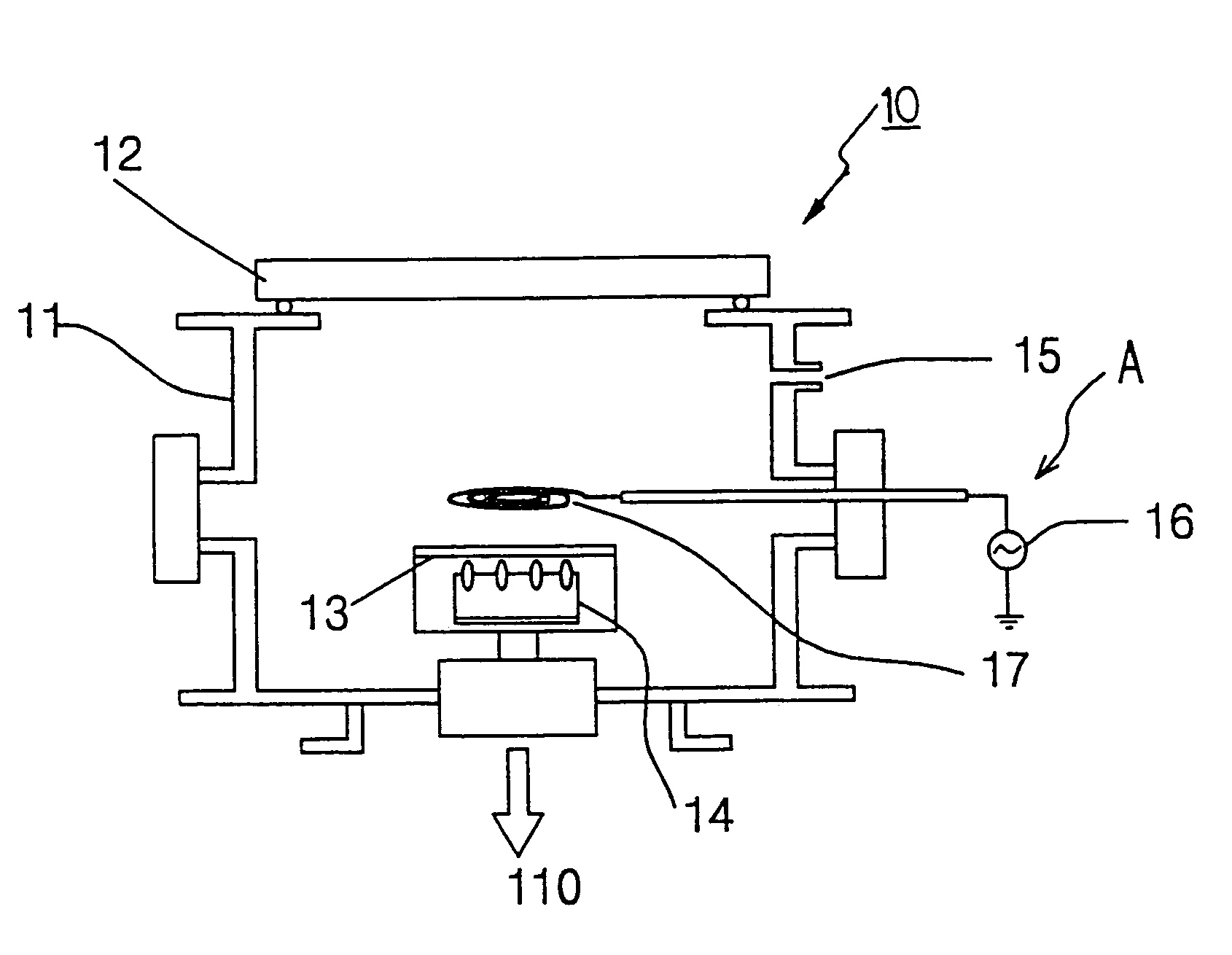
[0039]A method of crystallizing an amorphous silicon layer according to the present invention is characterized by crystallizing amorphous silicon within a short period at low temperature without metal contamination by means of accelerating crystallization of the layer by using plasma.

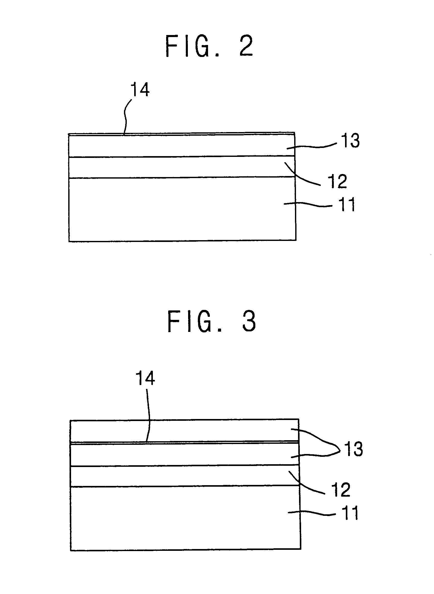
[0040]An amorphous silicon layer experiences crystallization by forming a semiconductor layer of amorphous silicon on an insulated substrate, such as quartz, glass, oxide or the like, by exposing the semiconductor layer to plasma generated by RF power or DC power and by carrying out annealing with the presence of plasma, successively. Plasma induces silicon crystallization by having metal atoms inside a reaction chamber deposited on the amorphous silicon layer. In order to have specific metal deposited on the amorphous silicon layer as a plasma-...


PUM

PropertyMeasurementUnit
Temperatureaaaaaaaaaa
Shapeaaaaaaaaaa

Abstract

The present invention is related to a method of crystallizing an amorphous silicon layer and a crystallizing apparatus thereof which crystallize an amorphous silicon layer using plasma. The present invention includes the steps of depositing an inducing substance for silicon crystallization on an amorphous silicon layer by plasma exposure, and carrying out annealing on the amorphous silicon layer to the amorphous silicon layer. The present invention includes a chamber having an inner space, a substrate support in the chamber wherein the substrate support supports a substrate, a plasma generating means in the chamber wherein the plasma generating means produces plasma inside the chamber, and a heater at the substrate support wherein the heater supplies the substrate with heat.

Description

[0001]This application is a continuation of prior application Ser. No. 09 / 350,313, filed Jul. 9, 1999 now U.S. Pat. No. 6,816,059.[0002]This application claims the benefit of Korean Patent Application Nos. 98-27716 filed Jul. 10, 1998 and 98-44230 filed on Oct. 21, 1998, which is hereby incorporated by reference.BACKGROUND OF THE INVENTION[0003]1. Field of Invention[0004]The present invention relates to a method of crystallizing an amorphous silicon layer and a crystallizing apparatus thereof in which the amorphous silicon layer is crystallized by using plasma.[0005]2. Discussion of Related Art[0006]In view of performance, low temperature polysilicon, of which product cost is low owing to its low formation temperature and which also provides wide image area, is as good as high temperature polysilicon. There are various methods for forming low temperature polysilicon, such as solid phase crystallization, laser crystallization and the like.[0007]When providing low temperature crystall...

Claims


Application Information

Patent Timeline
IPC IPC(8): C30B25/14C30B1/02H01L21/20
CPCC30B1/023H01J37/32009H01L21/2022C30B29/06Y10T117/10Y10T117/1008H01L21/02422H01L21/02532H01L21/02505H01L21/0245H01L21/02609H01L21/0242H01L21/02672H01L21/02595
Inventor JANG, JINYOON, SOO-YOUNGOH, JAE-YOUNGSHON, WOO-SUNGPARK, SEONG-JIN
Owner JANG JIN
Why Eureka
Try Eureka