Semiconductor package, semiconductor device and electronic device

a semiconductor and semiconductor technology, applied in the field of semiconductor devices and electronic devices, can solve the problems of increased production costs, difficult control of the height of metal posts, and long time-consuming, and achieve the effects of reducing production costs, ensuring electric conduction and adhesive strength, and reducing production costs

Inactive Publication Date: 2006-04-04
THE FUJIKURA CABLE WORKS LTD +1
View PDF22 Cites 53 Cited by
  • Summary
  • Abstract
  • Description
  • Claims
  • Application Information

AI Technical Summary

Benefits of technology

[0011]In the present invention, the post is provided with the resin projection portion wherein at least the upper surface thereof is coated with the conductive layer. Therefore, in the case that stress is generated in this post, the stress is dispersed mainly by the resin projection portion. For this reason, no thick plating layer is necessary for the post, so that the production process is shortened. Since the height of the post can be controlled by the height of the resin projection portion, the adjustment thereof is easy.
[0012]By making an area of the opening portion made in the sealing resin layer through which the post penetrates larger than that of the upper surface of the post, the contact area between the solder bump and the conductive layer can be made large. Therefore, the reliability of ensuring electric conduction and adhesive strength is improved. In this case, a boundary between the post and the sealing resin layer may be present outside the upper surface of the post as is viewed in plan.
[0013]In the case that the inner surface of the opening portion made in the sealing resin layer is inclined inwards to form a groove surrounding a periphery of the upper surface of the post and the boundary is divided by the groove, the flexibility of the deformation of the resin projection portion becomes large on the basis of resin-removal. Thus, the stress is still more easily dispersed.
[0014]In the case that at least one part of a periphery of the post is coated with the sealing resin layer and the sealing resin layer is formed to have such a thickness that its upper surface apart from the post is lower than the upper surface of the post, the flexibility of the deformation of the resin projection portion becomes large in the same way. Thus, the stress is still more easily dispersed.

Problems solved by technology

However, if a metal post having such a height is formed by plating, there is a problem that a remarkable long period of time is required.
This further gives rise to the problems of increased production cost and a difficulty in control of the height of the metal post.

Method used


Image

  • Semiconductor package, semiconductor device and electronic device
  • Semiconductor package, semiconductor device and electronic device
  • Semiconductor package, semiconductor device and electronic device

Examples


Embodiment Construction

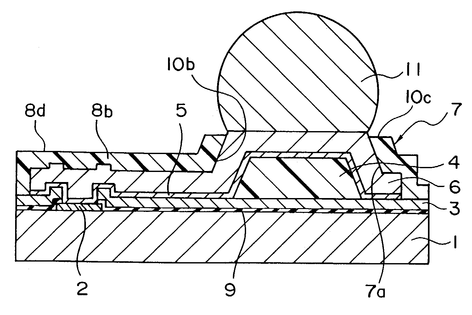
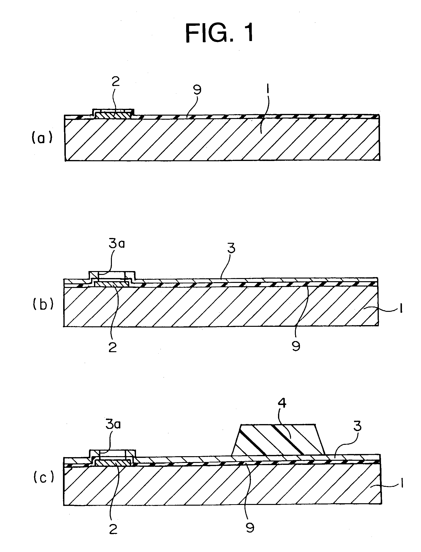
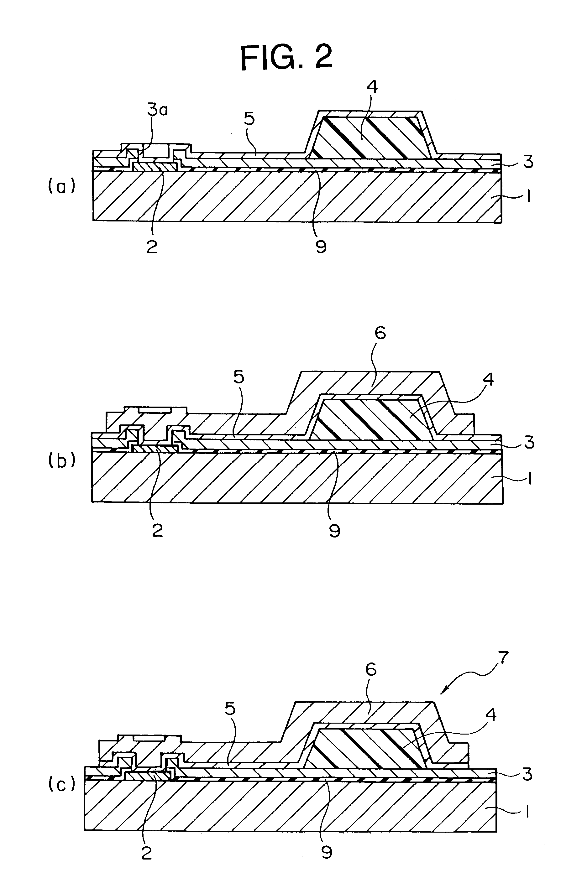
[0033]A method for producing a semiconductor package according to embodiments of the present invention will be hereinafter explained in detail with reference to the appended drawings. FIGS. 1(a) to (c), FIGS. 2(a) to (c), and FIGS. 3(a) and (b) are sectional views showing a method for producing a semiconductor package according to a first embodiment of the present invention in step order.

[0034]In the present embodiment, as shown in FIG. 1(a), there is first prepared a product wherein a passivation film 9, made of SiN or the like, is directly formed on the entire surface of a Si wafer 1 in which an integrated circuit (not shown) and electrodes thereof, for example, an Al pad 2, are disposed. An opening portion is made at the position conformable to the Al pad 2 in the passivation film 9, so that the Al pad 2 is exposed.

[0035]Thereafter, as shown in FIG. 1(b), an insulating layer 3 made of a resin and having an opening portion 3a at the position conformable to the Al pad 2 is formed. ...


PUM


Abstract

An insulating layer (3) having an opening portion (3a) at a position conformable to an electrode pad (2) is formed. Next, a resin projection portion (4) is formed on the insulating layer (3). Thereafter, a resist film is formed which has opening portions made in regions conformable to the opening portion (3a), the resin projection portion (4) and the region sandwiched therebetween. A Cu plating layer (6) is formed by electrolytic copper plating, using the resist film as a mask.

Description

TECHNICAL FIELD[0001]The present invention relates to a semiconductor package, such as a wafer level CSP (Chip Size / Scale Package), using no wiring board (interposer), a semiconductor device, an electronic device, and a method for producing the semiconductor package; and particularly to a semiconductor package, a semiconductor device and an electronic device which can be produced with ease, and a method for producing the semiconductor package.BACKGROUND ART[0002]In recent years, a development of small-sized semiconductor devices has been promoted. With this development, attention is paid to the miniaturization of the packages of these semiconductor devices. For instance, a variety of semiconductor packages have been proposed in the August issue (1998) and February issue (1999) of Nikkei Micro-device. Among these packages, especially a wafer level CSP using a semiconductor package called CSP has a high effect on the miniaturization of a package and a reduction in costs. This CSP is a...

Claims


Application Information

Patent Timeline
Patent Type & Authority Patents(United States)
IPC IPC(8): H01L23/48H01L21/56H01L23/31H01L23/485H01L23/525
CPCH01L21/56H01L23/3107H01L24/13H01L23/3114H01L23/525H01L24/10H01L2924/0002H01L2224/0401H01L2224/0231H01L2224/13099H01L2924/01004H01L2924/01013H01L2924/01015H01L2924/01022H01L2924/01029H01L2924/01033H01L2924/01078H01L2924/01079H01L2924/10329H01L2924/14H01L2924/15311H01L2224/05567H01L2224/13021H01L2224/13023H01L2924/01005H01L2924/01006H01L2924/01024H01L2924/014H01L2224/05572H01L2924/00H01L2224/05552H01L2224/13022H01L2224/13H01L2224/05124H01L2224/05147H01L2224/05155H01L2224/05166H01L2224/05171H01L2224/05644H01L2224/02351H01L2224/02125H01L2224/05548H01L2224/0236H01L24/03H01L24/05H01L2924/0001H01L2224/02377H01L2224/13024H01L24/02H01L2924/00014H01L2224/02
Inventor SUZUKI, TAKANAOINABA, MASATOSHIOMINATO, TADANORIKAIZU, MASAHIROKUROSAKA, AKIHITOSADAKATA, NOBUYUKIMASUMOTO, MUTSUMIMASUMOTO, KENJI
Owner THE FUJIKURA CABLE WORKS LTD
Why Eureka
Try Eureka