Method for reducing wafer arcing

a technology of arcing and wafers, applied in the direction of electrostatic holding devices, semiconductor/solid-state device testing/measurement, instruments, etc., can solve the problems of device destruction, yield loss of product wafers, general drive of negative wafer potential, etc., and achieve the effect of reducing the arcing of wafers in the etching operation

Active Publication Date: 2006-04-11
LAM RES CORP
View PDF10 Cites 36 Cited by
  • Summary
  • Abstract
  • Description
  • Claims
  • Application Information

AI Technical Summary

Benefits of technology

[0009]Broadly speaking, the present invention fills these needs by providing a method for reducing wafer arcing in wafer etching operations. It should be appreciated that the present invention can be implemented in numerous ways, including as a process, an apparatus, a system, a device or a method. Several inventive embodiments of the present invention are described below.
[0010]In one embodiment, a method for reducing wafer damage during an etching process is provided. In one of the many embodiments, the method includes assigning a bias voltage to each of at least one etching process, and generating the assigned bias voltage before initiation of one of the at least one etching process. The method further includes applying the assigned bias voltage to an electrostatic chuck before initiation of one of the at least one etching processes. The assigned bias voltage level reduces wafer arcing.
[0011]In yet another embodiment, a method for reducing wafer damage during an etching process is provided. The method includes generating a recipe bias table that includes associations between at least one bias voltage and at least one etching process where each one of the at least one etching process corresponding to the at least one bias voltage. The method also includes determining an etching process to be conducted, and matching the etching process to a corresponding bias voltage by using the associations in a recipe table. The method further includes generating one of the at least one bias voltage corresponding to the etching process. The method also includes applying the one of the at least one bias voltage to an electrostatic chuck (ESC) before initiation of the etching process. The one of the at least one bias voltage reduces arcing in a wafer during the etching process.
[0014]The advantages of the present invention are numerous. Most notably, by creating a method of associating bias voltages applied to the electrostatic chuck (ESC) with different wafer etching processes, the bias voltages may be intelligently set to a particular bias voltage before each particular etching stage. In this way, each etching process that could generate a different voltage potential between a surface of the wafer and substrate can be compensated for thereby reducing wafer arcing. Therefore, by adjusting and tailoring the bias voltage applied to the ESC to each specific etching process step, wafer arcing can be reduced in an effective manner. Therefore, advantageously, this method enables the use of multiple etching chemistries and etch chamber conditions so that different etching operations may be used without the problems of arcing. This may result in a more controlled etching process. Additionally, because wafer damage can be decreased dramatically, the wafer yield loss can be decreased.

Problems solved by technology

As a result of this enhanced complexity in chip manufacturing plasma induced damage may occur more frequently leading to device destruction and, therefore, to yield losses on a product wafer.
However, as soon as plasma is struck, the wafer potential is generally driven to a negative value with respect to the chamber walls within a few dozen RF cycles.
This, however, may lead to arcing on the wafer, since the ESC power supply is too slow to follow fast voltage changes on the wafer surface as they occur, for instance, during plasma ignition.
When the voltage differential between adjacent metal structures within the dielectric of the wafer exceeds the electrical breakdown strength of that dielectric, arcing will occur, leading to damage or destruction of the structures within the dielectric layer.
In most cases, this will render the wafer unusable even though only as little as one die on the wafer may have been affected by the arcing.
Consequently, if such occurrences are allowed to happen, wafer yields would be decreased and wafer production costs would increase.
Unfortunately, in this circumstance, the surface potential 42 increases too quickly for the compensation circuit of the ESC power supply.
Therefore the substrate potential cannot be adjusted in a timely response to the surface potential increase.
Therefore, wafer arcing as is described in reference to FIG. 1A may occur thereby damaging the wafer and decreasing wafer production yield and efficiency.

Method used


Image

  • Method for reducing wafer arcing
  • Method for reducing wafer arcing
  • Method for reducing wafer arcing

Examples


Embodiment Construction

[0027]An invention is disclosed for a method to intelligently decreasing wafer arcing during etch procedures and other procedures such as, for example, deposition procedures or whenever there is a process where plasma interacts with a wafer and a bias compensation is needed. In the following description, numerous specific details are set forth in order to provide a thorough understanding of the present invention. It will be understood, however, by one of ordinary skill in the art, that the present invention may be practiced without some or all of these specific details. In other instances, well known process operations have not been described in detail in order not to unnecessarily obscure the present invention.

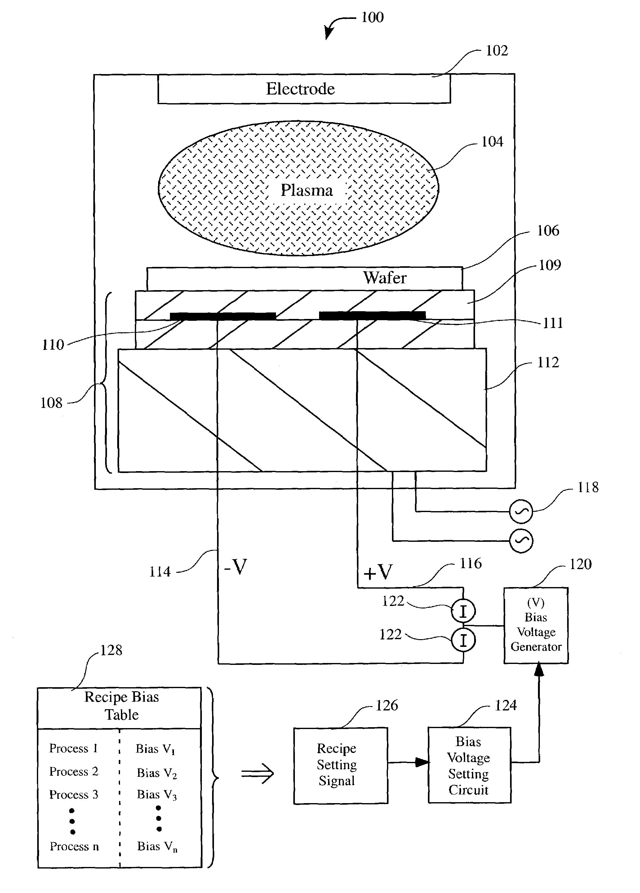
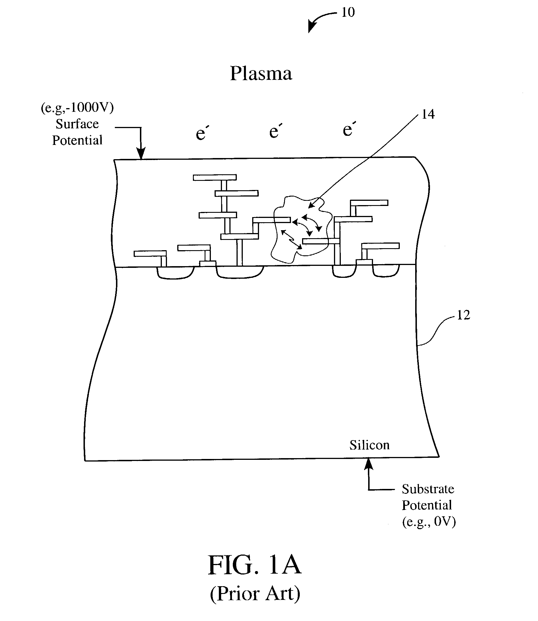
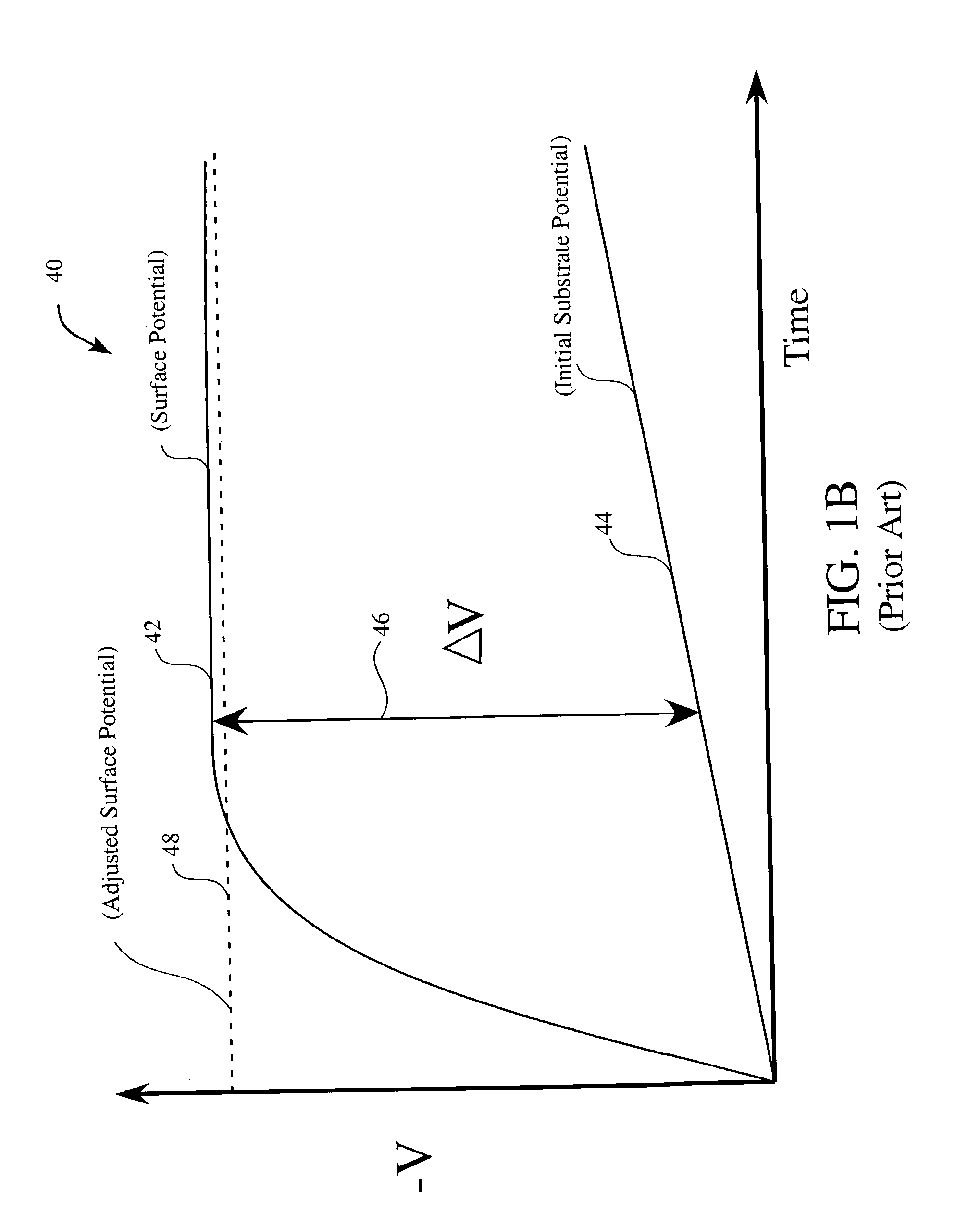
[0028]In general terms, the present invention is directed toward a method whereby an etch process may be utilized with a dramatic reduction in arcing between structures of the wafer, between a structure and the substrate, or between a structure and the plasma. This may be acc...


PUM


Abstract

A method for reducing wafer damage during an etching process is provided. In one of the many embodiments, the method includes assigning a bias voltage to each of at least one etching process, and generating the assigned bias voltage before initiation of one of the at least one etching process. The method further includes applying the assigned bias voltage to an electrostatic chuck before initiation of one of the at least one etching processes. The assigned bias voltage level reduces wafer arcing.

Description

BACKGROUND OF THE INVENTION[0001]1. Field of the Invention[0002]The present invention relates to wafer processing methods and, more particularly, to efficient and cost effective etch operations for wafers.[0003]2. Description of the Related Art[0004]Modern microchip designs have been trending toward ever more complicated chip structures and toward increased numbers of processing steps for a single chip. In particular, the number of interconnected metal layers stacked on top of each other has grown continuously over the past. With it, the number of plasma processing steps and the amount of thermal and electric stress each wafer incurs during its processing have increased as well. As a result of this enhanced complexity in chip manufacturing plasma induced damage may occur more frequently leading to device destruction and, therefore, to yield losses on a product wafer.[0005]In typical wafer etching operations, the wafer is clamped by an electrostatic chuck (ESC) so that the wafer does...

Claims


Application Information

Patent Timeline
Patent Type & Authority Patents(United States)
IPC IPC(8): H01L21/66H01L21/3065H02N13/00H01L21/00H01L21/311H01L21/683
CPCH01L21/6831H01L21/67069H01L21/31116H01J2237/0206H01L21/311
Inventor FISCHER, ANDREAS
Owner LAM RES CORP
Why Eureka
Try Eureka