Reticle with antistatic coating

a technology of anti-static coating and reticle, which is applied in the field of semiconductor industry, can solve the problems of uncontrolled electrostatic discharge (esd), especially prone to static electrical charges, and geometry degradation, and achieve the effect of eliminating the potential damage of esd

Inactive Publication Date: 2006-04-18
TAIWAN SEMICON MFG CO LTD
View PDF1 Cites 13 Cited by
  • Summary
  • Abstract
  • Description
  • Claims
  • Application Information

AI Technical Summary

Benefits of technology

[0010]A primary object of the present invention is to provide an antistatic protection for a reticle that would be compatible with existing reticle-pellicle structure and where potential damage from ESD would be eliminated.

Problems solved by technology

Due to specific conditions accompanying semiconductor-manufacturing process, namely low humidity (typically 40%±10% RH), it is especially prone to developing static electrical charges.
Accumulated on the chrome, electrostatic charge leads to an uncontrolled electrostatic discharge (ESD), one of the key causes of geometry degradation.
Specifically, depositing its energy into a very small area of the wafer, ESD irreversibly damages the latter literally vaporizing metal conductor lines.
Instances of these effects can result in the non-functioning of IC devices created from the degraded photomask.

Method used


Image

  • Reticle with antistatic coating
  • Reticle with antistatic coating
  • Reticle with antistatic coating

Examples


Embodiment Construction

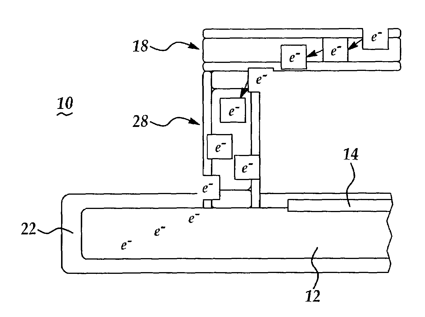
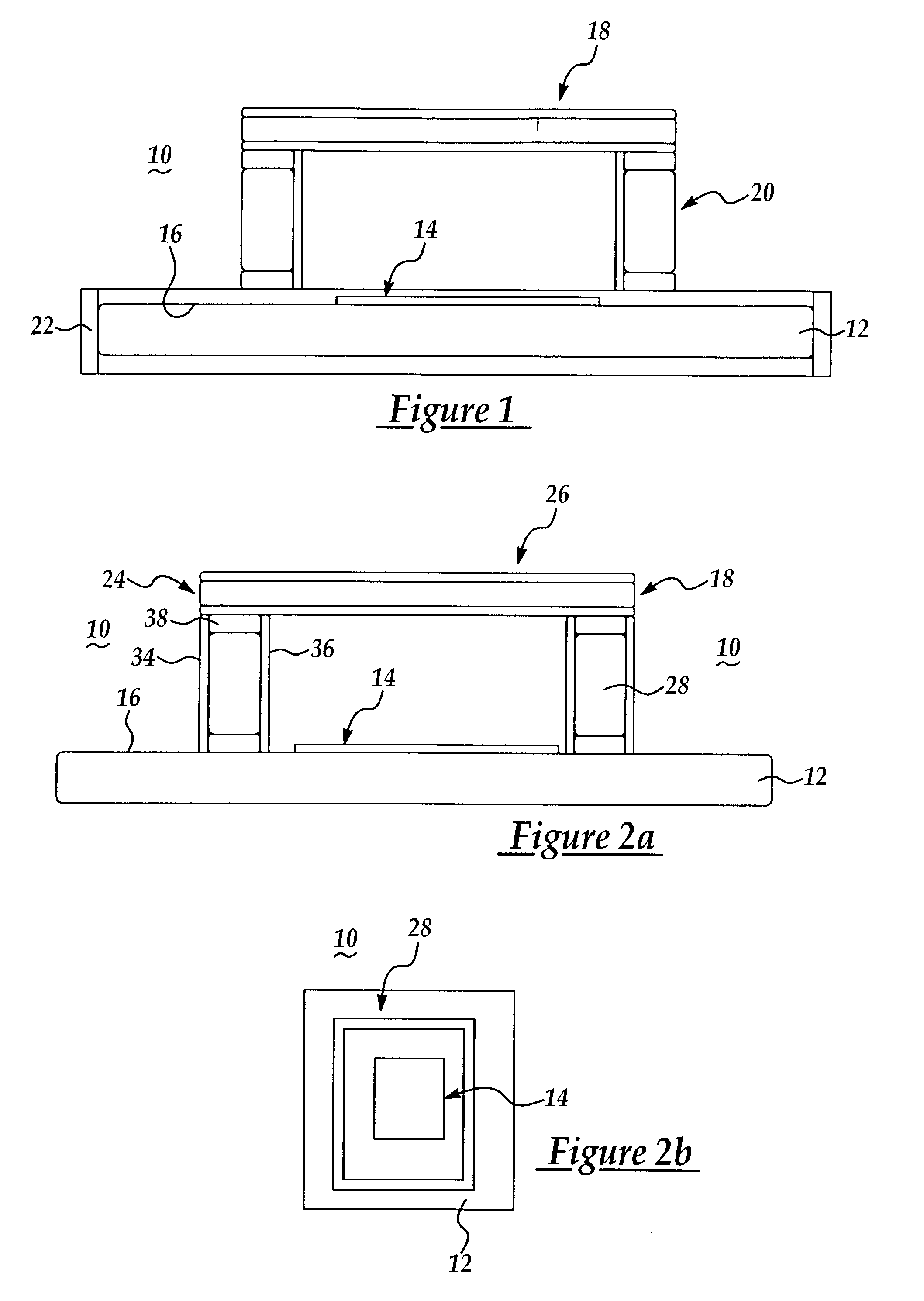
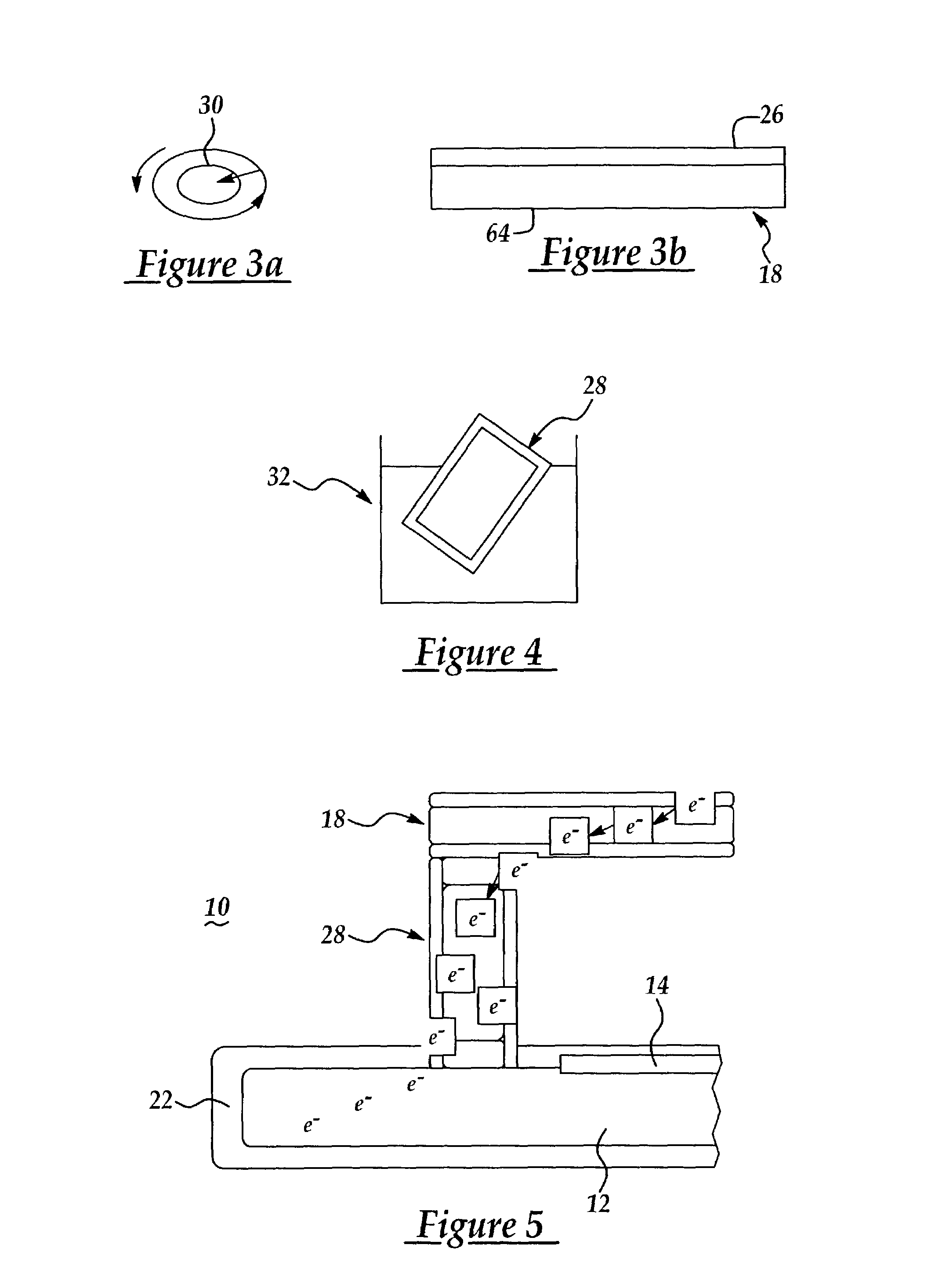
[0041]Referring now to FIG. 1, a photomask (reticle) 10 has a quartz blank 12 with a thin patterned opaque metal layer 14, preferably made of chromium (chrome), deposited on a surface 16 of the blank 12. Typically, the layer 14 is formed with chrome less than 100 nm thick and covered with an anti-reflective coating, such as chrome oxide (not shown). A pellicle membrane 18 is arranged over the layer 14 of the reticle to keep it free of foreign particles. A frame 20, over which the membrane 18 is tightly stretched, allows positioning the latter at some height above the photomask. Such height (usually, of about 5–10 mm) is greater than the focal length of the light imaged onto the photomask. Thus, a dust particle that found its way on the pellicle is out of focal plane and is invisible to the projection optics. A conventional pellicle frame is made of anodized aluminum.

[0042]According to the present invention, a layer 22 of an antistatic film is deposited onto the reticle 10. The layer...


PUM

PropertyMeasurementUnit
thicknessaaaaaaaaaa
widthaaaaaaaaaa
widthaaaaaaaaaa

Abstract

A static resistant reticle comprises a substrate and a patterning layer and is covered by an antistatic conductive film of quaternary amine (R4N)+Cl. A pellicle structure comprising an optically transparent membrane tightly stretched on a frame is also coated by an antistatic electro conductive film of a similar material. The reticle with the pellicle form a shielded structure isolating the reticle from ESD.

Description

BACKGROUND OF THE INVENTION[0001]1. Field of the Invention[0002]The present invention relates to semiconductor industry, more particularly to reticles used in microlithography, and still more particularly to reticles with a thin film coating to isolate the mask from electric static field.[0003]2. Description of the Related Art[0004]A microlithography (or photolithography) process for manufacturing a semiconductor device comprises a photoresist application process, an exposure process, and a development process. During the photolithography process, semiconductor manufacturers often use a photomask to copy an image of an electronic circuit onto a semiconductor wafer. Photomasks come in various sizes and shapes such as 1X and 2X photomasks or 2X, 2.5X, 4X, and 5X reticles. Depending on the reduction factor X, line width and line space geometries for a resulting semiconductor device are from less than 10 microns to less than 2 microns. Other mask line spacings and semiconductor line spa...

Claims


Application Information

Patent Timeline
Patent Type & Authority Patents(United States)
IPC IPC(8): G03F9/00A47G1/12B44F1/00G03F1/40G03F1/48G03F1/64G03G16/00
CPCG03F1/40G03F1/64G03F1/48
Inventor SU, WEI-YUCHENG, DONG-HSUTURN, LI-KONG
Owner TAIWAN SEMICON MFG CO LTD
Why Eureka
Try Eureka