Semiconductor device with multiple power sources

a technology of semiconductor and power source, applied in pulse generators, pulse techniques, instruments, etc., can solve the problems of disadvantageous increase of manufacturing cost, large leak current (large off-leak current), and disadvantageous increase of standby current in control circuit ctl in dram macro dm, so as to reduce both manufacturing cost and standby current

Inactive Publication Date: 2006-04-18
RENESAS TECH CORP
View PDF10 Cites 48 Cited by
  • Summary
  • Abstract
  • Description
  • Claims
  • Application Information

AI Technical Summary

Benefits of technology

[0043]It is an object of the present invention to provide a semiconductor device with multiple power sources, capable of reducing both manufacturing cost and standby current.
[0044]It is another object of the present invention to provide a semiconductor device with multiple power sources, capable of reliably causing no latch-up phenomenon irrespectively of a power application sequence.
[0045]It is a specific object of the present invention to provide an embedded memory capable of reducing manufacturing cost and standby current and preventing the occurrence of a latch-up phenomenon irrespectively of a power application sequence.

Problems solved by technology

Therefore, the MOS transistor in logic LG causes a large leak current (large off-leak current) when being turned off.
However, if the MOS transistor having the absolute value of the threshold voltage different from that of the logic transistor is used in control circuit CTL, it is necessary to manufacture the logic transistor of logic LG and the MOS transistor of control circuit CTL in individual different manufacturing steps, which disadvantageously increases manufacturing cost.
Thus, the logic transistor is used as the MOS transistor for control circuit CTL, and therefore, the standby current in control circuit CTL in DRAM macro DM disadvantageously increases and low current consumption cannot be achieved.
If this “latch-up phenomenon” occurs, a large current flows due to the thyristor operation of these parasitic bipolar transistors, and the MOS transistors may be destructed or a signal interconnection line may be cut off due to generated heat.
If such a latch-up phenomenon occurs, it is only possible to stop the thyristor operation by shutting off the supply of the power supply voltage.
However, it is impossible to instantly identify externally whether or not the latch-up phenomenon occurs internally.
As a result, the logic transistor cannot be used for the control circuit at the peripheral circuit of the DRAM macro and manufacturing cost cannot be reduced.
Besides, if the logic transistor is used for the DRAM peripheral control circuit, a well bias cannot be adjusted and therefore, the standby current cannot be reduced.

Method used


Image

  • Semiconductor device with multiple power sources
  • Semiconductor device with multiple power sources
  • Semiconductor device with multiple power sources

Examples


first embodiment

[First Embodiment]

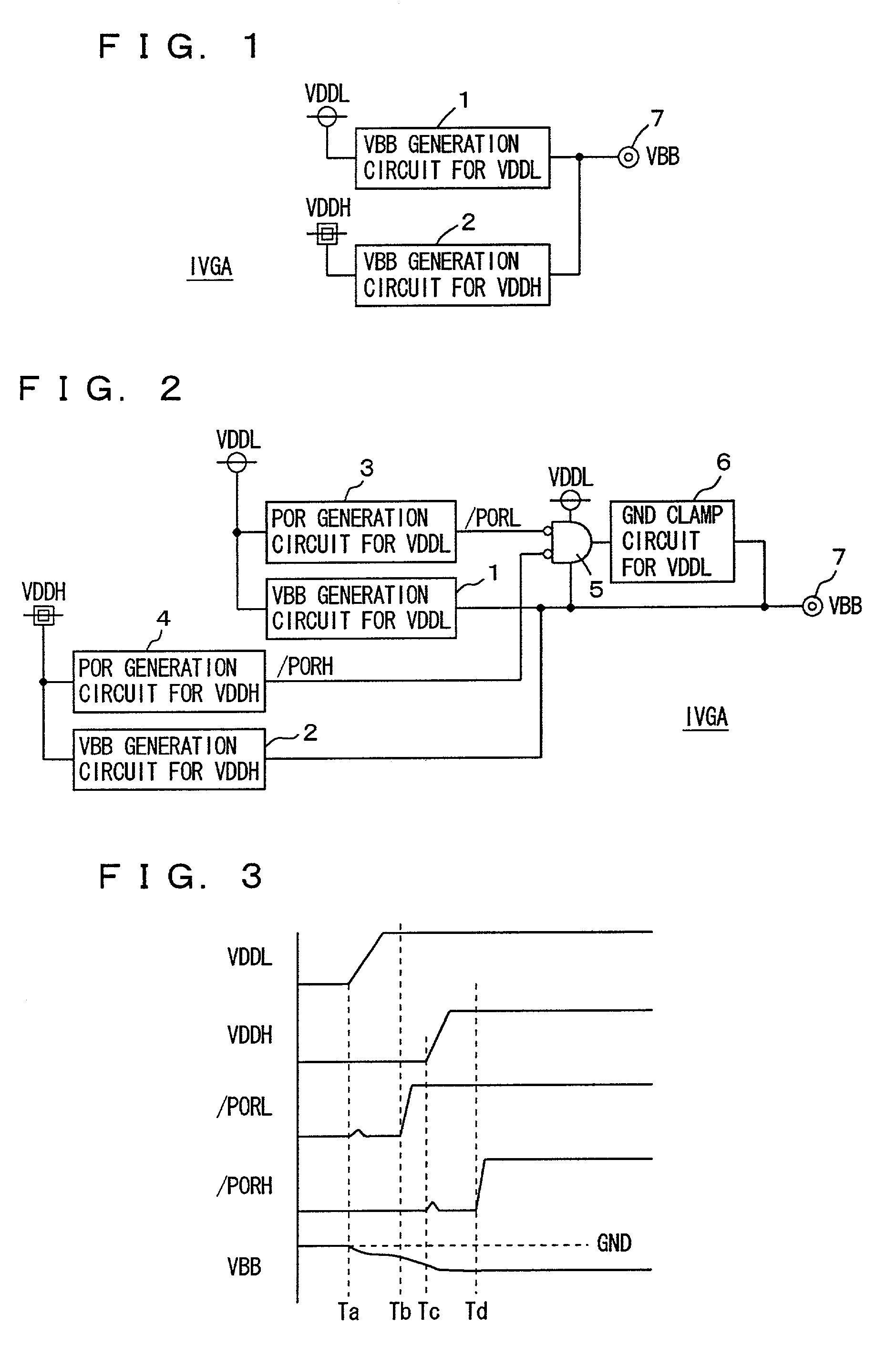
[0097]FIG. 1 is a schematic diagram showing the construction of the main portion of a semiconductor device in the first embodiment according to the present invention. In FIG. 1, the construction of internal voltage generation circuit IVGA included in embedded DRAM macro DM as shown in FIG. 36 is shown. In FIG. 1, internal voltage generation circuit IVGA includes a VBB generation circuit 1 for VDDL which generates negative voltage VBB in accordance with logic power supply voltage VDDL, and a VBB generation circuit 12 for VDDH which generates negative voltage VBB in accordance with memory power supply voltage VDDH.

[0098]VBB generation circuits 1 and 2 are merely required to generate negative voltage VBB applied to the same region. Negative voltage VBB may be applied to the substrate region of memory array MA as shown in FIG. 36 and may be different in voltage level from a substrate bias voltage applied to memory array MA. What is necessary is that negative voltage VB...

second embodiment

[Second Embodiment]

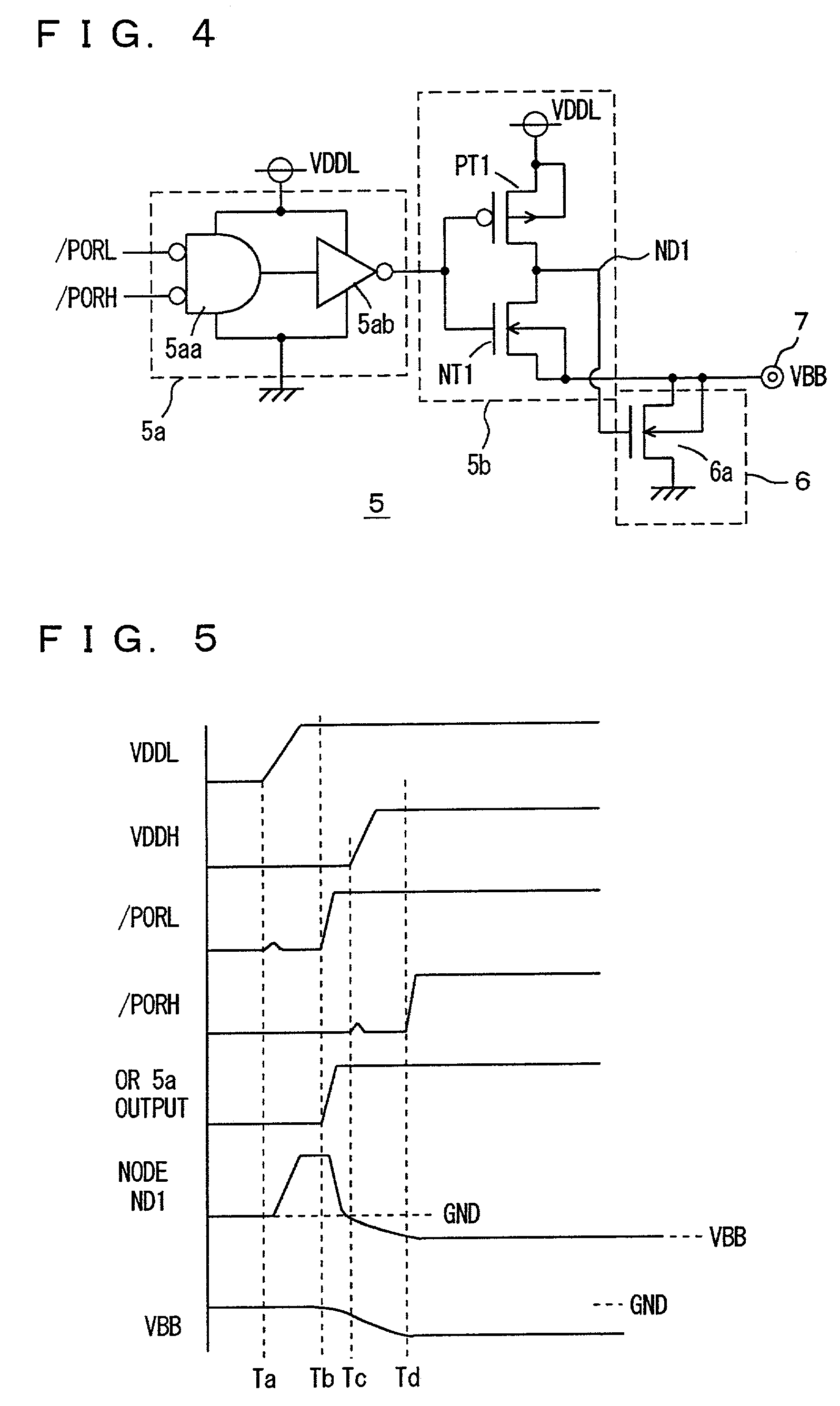
[0102]FIG. 2 is a schematic diagram showing the construction of an internal voltage generation circuit in the second embodiment according to the present invention. In FIG. 2, internal voltage generation circuit IVGA includes the following components, in addition to VBB generation circuit 1 for VDDL and VBB generation circuit 2 for VDDH described in the first embodiment. Specifically, internal voltage generation circuit IVGA includes a POR generation circuit 3 for VDDL which detects the application of logic power supply voltage VDDL and generates a power on detection signal (power on reset signal) / PORL kept at L level or in an active state for a predetermined period of time, a POR generation circuit 4 for VDDH which detects the application of memory power supply voltage VDDH and generates a power on detection signal (power on reset signal) / PORH kept at an L level for a predetermined period of time when memory power supply voltage VDDH is applied or powered up, an ...

third embodiment

[Third Embodiment]

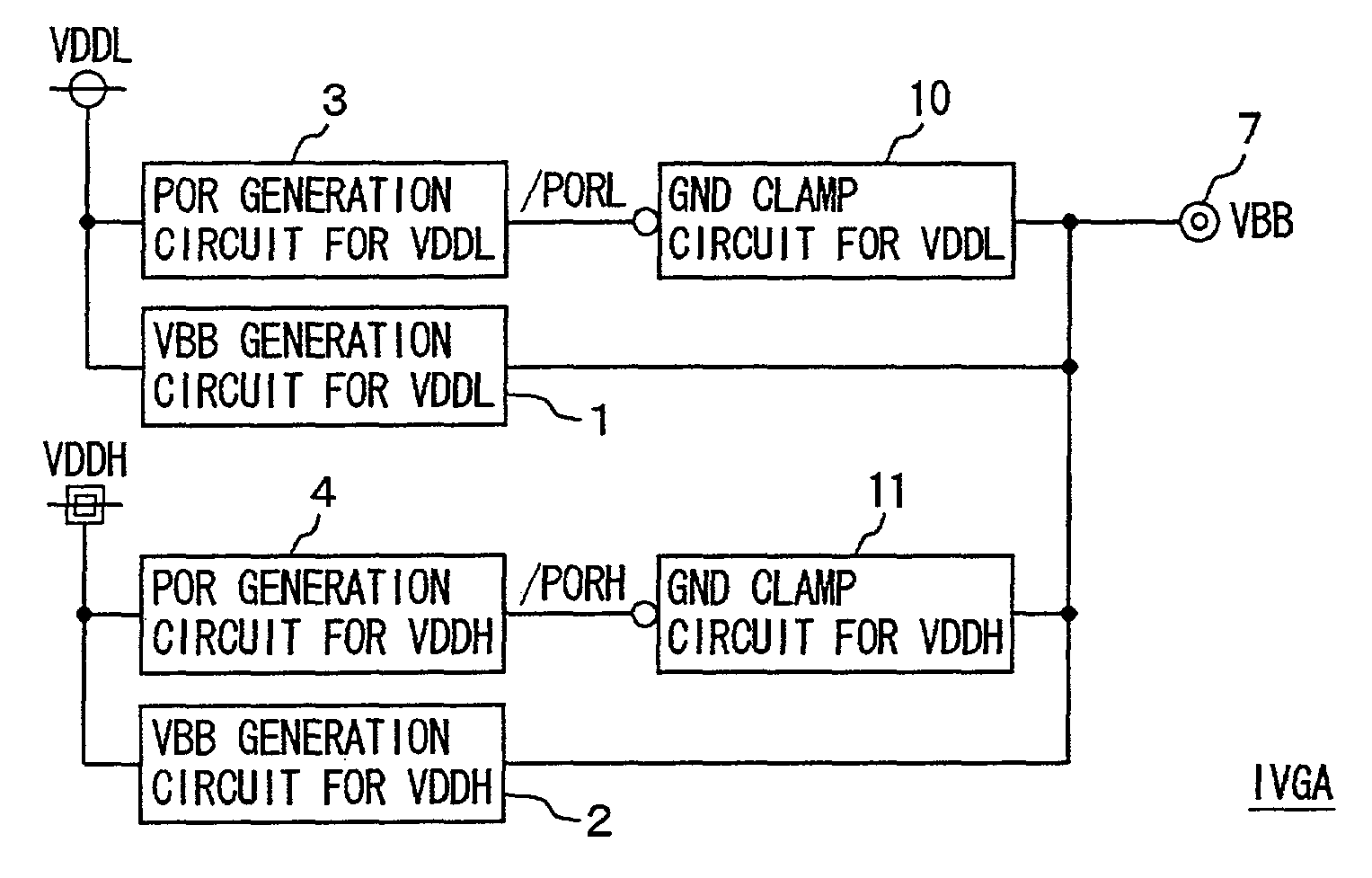
[0138]FIG. 8 is a schematic diagram showing the construction of an internal voltage generation circuit in the third embodiment according to the present invention. In the construction shown in FIG. 8, the internal voltage generation circuit includes a GND clamp circuit 10 for VDDL which clamps the voltage level of negative voltage output node 7 to the ground voltage level in accordance with logic power on detection signal / PORL applied from POR generation circuit 3 for VDDL, and a GND clamp circuit 11 for VDDH which clamps the voltage level of substrate bias voltage output node 7 to the ground voltage level in accordance with memory power on detection signal / PORH applied from POR generation circuit 4 for VDDH. Namely, in the construction shown in FIG. 8, GND clamp circuits for clamping the voltage level of the negative voltage output node 7 to the ground voltage level in accordance with logic power supply voltage VDDL and memory power supply voltage VDDH, respectiv...


PUM


Abstract

Well bias voltages are generated in accordance with a logic power supply voltage and a memory power supply voltage. The transistor included in a control circuit in a memory core is constituted of a logic transistor manufactured through the same manufacturing steps as those for the transistors of a logic formed on the same semiconductor substrate. Well bias voltages (VBB, VPP) are applied to a back gate of this logic transistor. A memory integrated with a logic on a common semiconductor substrate is provided which allows a transistor of a control circuit therein to be manufactured through the same manufacturing process as that of the logic and allows reduction of current consumption.

Description

BACKGROUND OF THE INVENTION[0001]1. Field of the Invention[0002]The present invention relates to a semiconductor device and particularly relates to a semiconductor device with a multiple power sources, which is operated with a plurality of power sources. More specifically, the present invention relates to an embedded memory integrated on a common semiconductor chip with a logic circuit. More particularly, the present invention relates to the construction of internal voltage generation circuitry of an embedded memory.[0003]2. Description of the Background Art[0004]Recently, system LSI's (large scale integrated circuits) each having a logic circuit and a large storage capacity DRAM (dynamic random access memory) integrated on the same semiconductor substrate are widely used.[0005]FIG. 36 is a schematic diagram showing a construction of a power source of a conventional system LSI. In FIG. 36, the system LSI includes a logic LG such as a processor and a DRAM macro DM serving as a main m...

Claims


Application Information

Patent Timeline
Patent Type & Authority Patents(United States)
IPC IPC(8): G05F1/10G11C11/408G11C5/14G11C11/407H01L21/822H01L27/04
CPCG11C5/146
Inventor YAMAZAKI, AKIRAMORISHITA, FUKASHITAITO, YASUHIKOFUJII, NOBUYUKIOKAMOTO, MAKO
Owner RENESAS TECH CORP
Why Eureka
Try Eureka