Versatile system for diffusion limiting void formation

a technology of diffusion limitation and void formation, which is applied in the direction of semiconductor devices, semiconductor/solid-state device details, electrical apparatus, etc., can solve the problems of stress-induced voids (sivs) around via structures, destroy electrical conductivity in devices, and fully comprehended, and achieves attractive metallization choice, low resistivity, and high melting point

Inactive Publication Date: 2006-04-25
TEXAS INSTR INC
View PDF9 Cites 11 Cited by
  • Summary
  • Abstract
  • Description
  • Claims
  • Application Information

AI Technical Summary

Benefits of technology

[0005]Among the new, alternative technologies being utilized, copper (Cu) and copper-based materials and technologies are gaining acceptance and preference for use in semiconductor device back-ends. Copper's relatively low resistivity and high melting point make it a particularly attractive metallizatio

Problems solved by technology

Because the use of copper based back-ends in semiconductor processing is still relatively immature, a number of physical properties and behaviors of copper, and the effects of those properties and behaviors on the performance of semiconductor devices, have yet to be fully comprehended.
One such problem that has become prevalent in devices utilizing such back-end technologies is the formation of stress-induced voids (SIVs) around via structures—particularly vias that are relatively isolated and located in proximity to relatively wide metallic interconnects.
The formation of such voids can destroy electrical conductivity in a device and present numerous and catastrophic device reliability problems.
Previously, the older, Al-based technologies often experienced very different void problems.
Such problems were most prevalent in relatively narrow metallic interconnects.
Voids wou

Method used


Image

  • Versatile system for diffusion limiting void formation
  • Versatile system for diffusion limiting void formation
  • Versatile system for diffusion limiting void formation

Examples


Embodiment Construction

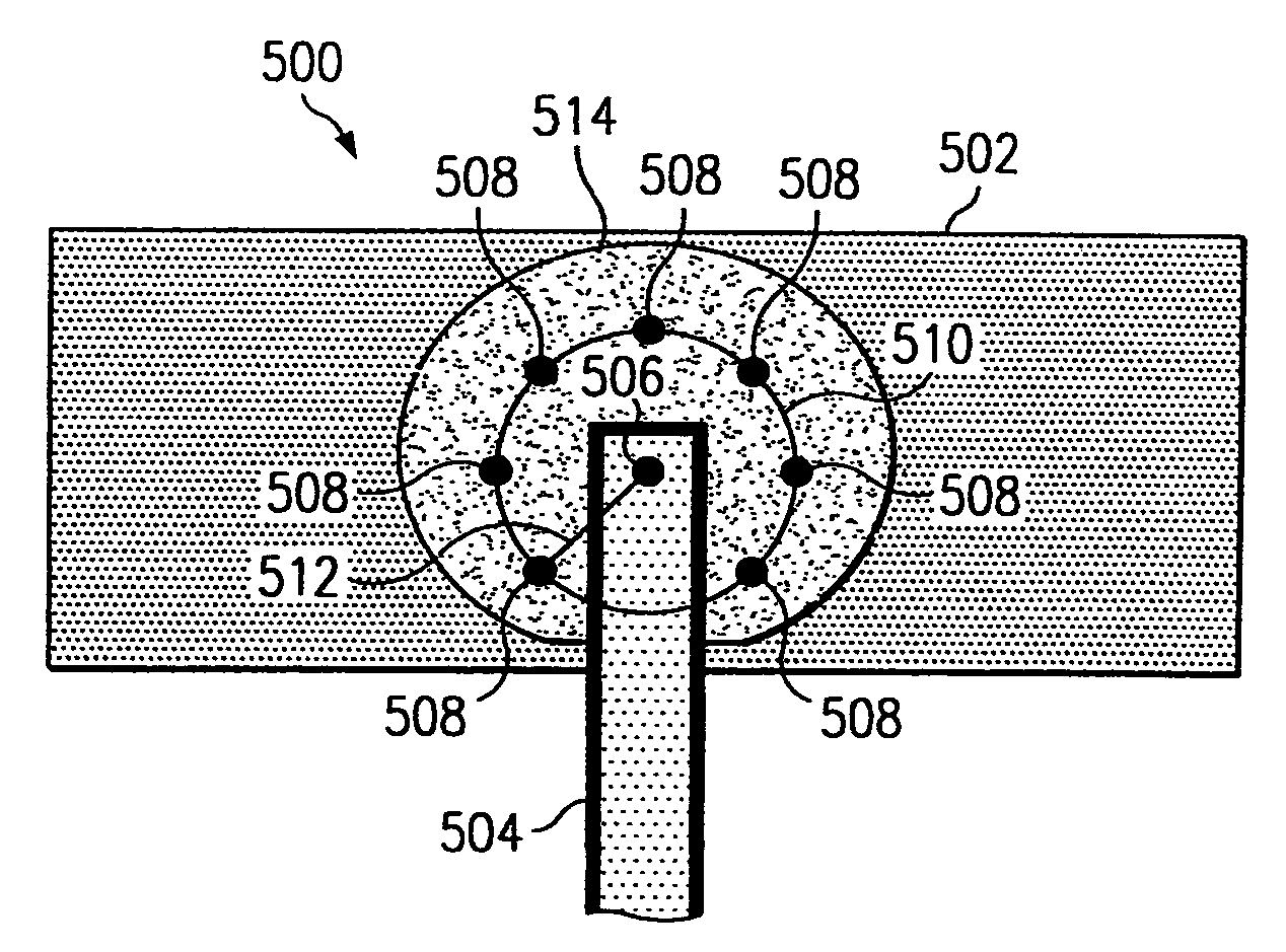
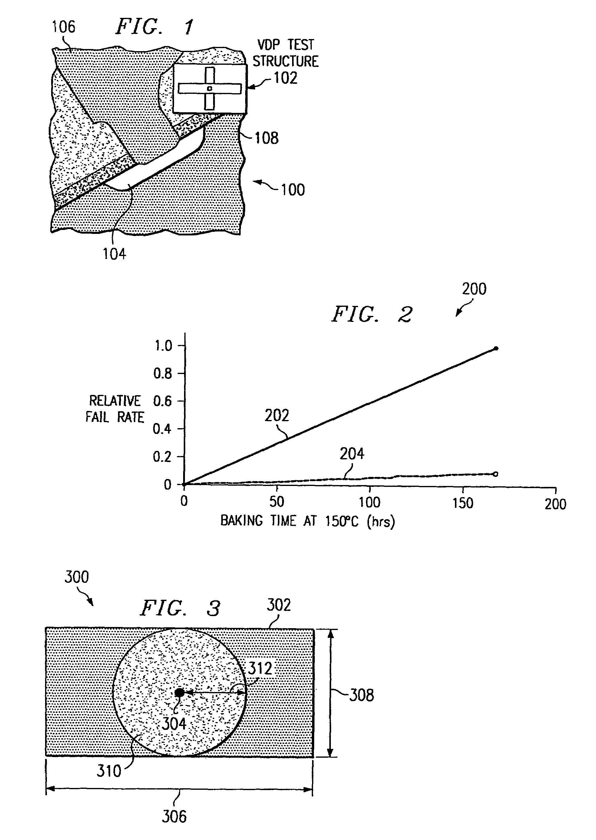
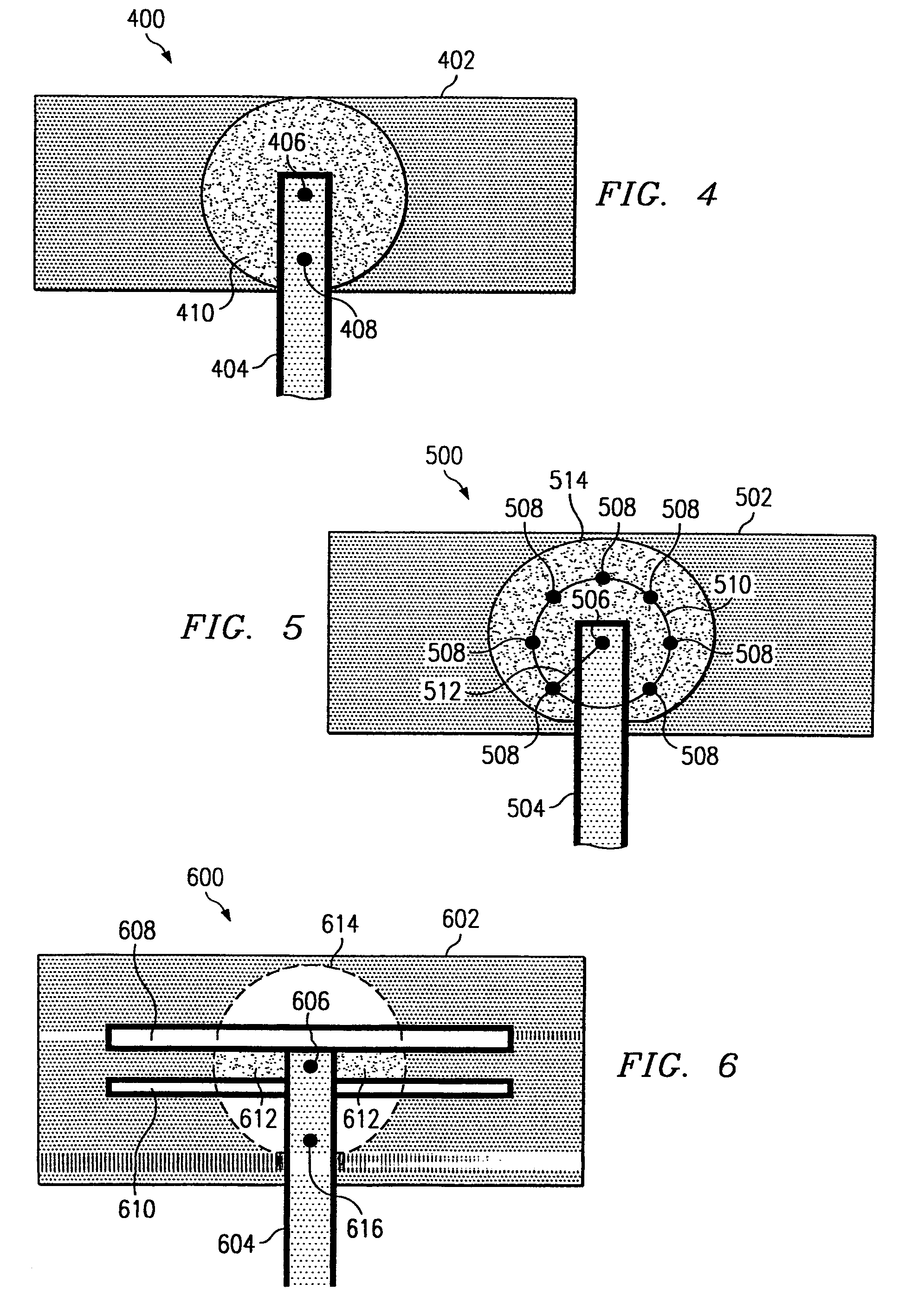
[0021]The present invention defines a system, comprising various structures and methods, for minimizing or eliminating the effects of stress-induced voiding in dual-damascene interconnect structures. The present invention provides a via redundancy scheme, a metal interconnect modification scheme, and combinations of both schemes in an easily scalable system that may be readily adapted and integrated into a number of device fabrication processes.

[0022]It should be understood that the principles disclosed herein may be applied in a wide range of semiconductor processing applications. Specifically, the present invention may be applied to any number of situations where stress-induced voiding is caused by the diffusive migration of material vacancies toward a particular structural element—regardless of the particular materials utilized or structures being processed. For purposes of explanation and illustration, however, the present invention is hereafter described in reference to stress-...


PUM


Abstract

Disclosed is apparatus and method for decreasing diffusive damage effects to a primary structure (406, 506) within a semiconductor device (400, 500). The device typically comprises a first interconnect (402, 502), and a second interconnect (404, 504). The primary structure is disposed between the first and second interconnects to electrically intercouple them. An active diffusion volume (410, 514) is determined, within which the primary structure is located. A buffer structure (408, 508) is disposed upon the first interconnect in proximity to the primary structure and adapted to buffer the primary via structure from diffusive voiding occurring at a contact point between the primary structure and the first interconnect.

Description

CROSS REFERENCE TO PRIOR APPLICATIONS[0001]This application is a division of Ser. No. 10 / 113,504, filed Apr. 1, 2002 now U.S. Pat. No. 6,737,351, which claims priority based upon provisional application Ser. No. 60 / 344,479, filed Dec. 28, 2001.FIELD OF THE INVENTION[0002]The present invention relates in general to the fabrication and operation of semiconductor devices and, more particularly, to apparatus and methods for diffusion limiting voids formed in semiconductor device structures during fabrication and operation of the semiconductor device.BACKGROUND OF THE INVENTION[0003]The continual demand for enhanced integrated circuit performance has resulted in, among other things, a dramatic reduction of semiconductor device geometries, and continual efforts to optimize the performance of every sub-structure within a semiconductor device. A number of improvements and innovations in fabrication processes, material composition, and layout of the active circuit levels of semiconductor dev...

Claims


Application Information

Patent Timeline
IPC IPC(8): H01L21/4763H01L21/768H01L23/522H01L23/532
CPCH01L21/768H01L21/76838H01L23/53228H01L23/5226Y10S438/926H01L2924/0002H01L23/522H01L23/5283H01L2924/00
Inventor OGAWA, ENNIS T.MCPHERSON, JOE W.
Owner TEXAS INSTR INC
Why Eureka
Try Eureka