Method of manufacturing a plasma display panel with adsorbing an impurity gas
a technology of plasma display panel and impurity gas, which is applied in the manufacture of electrode systems, gas mixture absorption, electric discharge tube/lamps, etc., can solve the problems of prone to adsorption of a large amount of h, difficult to add impurities, and difficult to diffuse impurity gas in discharge gas in a controlled manner, etc., to achieve improved performance, lower voltage, and high luminance
- Summary
- Abstract
- Description
- Claims
- Application Information
AI Technical Summary
Benefits of technology
Problems solved by technology
Method used
Image
Examples
first exemplary embodiment
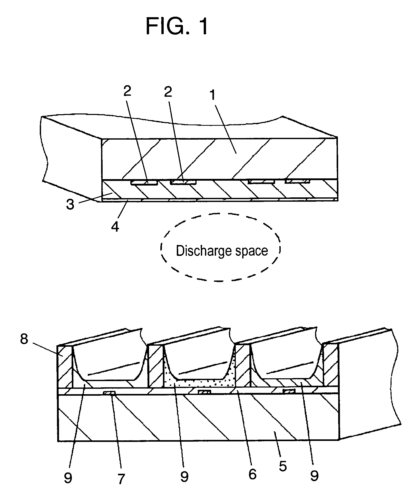
[0018]First, a description is provided of the first exemplary embodiment. FIG. 1 illustrates a structure of a PDP of the present invention. As shown in FIG. 1, a plurality of rows of stripe-like display electrodes 2, each made of a pair of a scan electrode and a sustain electrode, are formed on transparent substrate 1 made of material such as glass, on the front side. Dielectric layer 3 made of glass is formed so as to cover the electrodes. Formed on dielectric layer 3 is protective film 4 made of MgO.
[0019]On substrate 5 made of material such as glass, on the rear side, which is opposed to substrate 1 on the front side, a plurality of rows of stripe-like address electrodes 7 covered with visible light reflecting layer 6 made of dielectric glass are formed so as to intersect display electrodes 2, i.e. pairs of scan electrodes and sustain electrodes. On visible light reflecting layer 6 between these address electrodes 7, a plurality of ribs 8 are formed in parallel with address elect...
second exemplary embodiment
[0059]Next, the second exemplary embodiment is described.
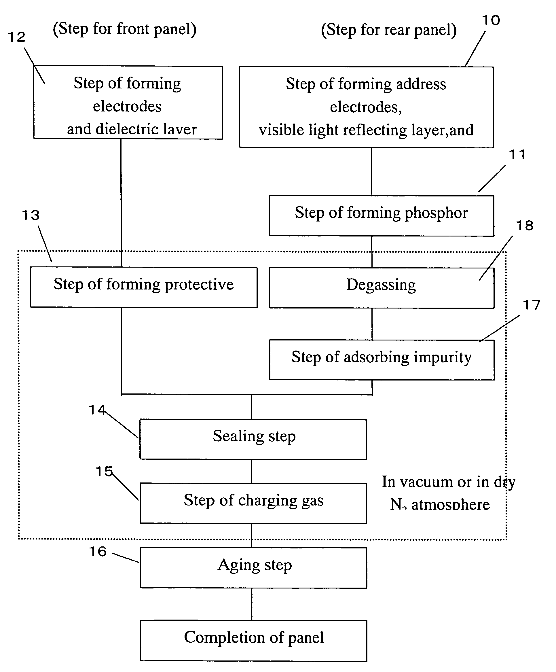
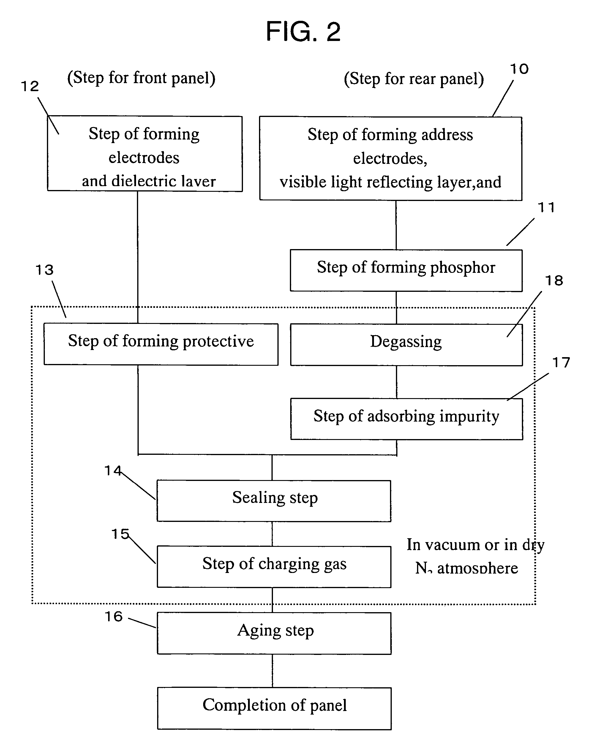
[0060]In the second exemplary embodiment, impurity gas containing at least CH4 is adsorbed by phosphor layers during or before the sealing step. Similar to the first exemplary embodiment, the impurity gas to be adsorbed is limited. For this purpose, glass substrates on front and rear sides are subjected to the steps surrounded by the dotted lines in FIG. 2 in a vacuum up to 10−4 Pa, or in a dry N2 atmosphere having a dew point up to −60° C. As for the glass substrate on the front side, all the steps from the formation of magnesium oxide, i.e. a protective film, by vacuum electron-beam evaporation to Step 15 of charging sealing gas are performed under the above conditions. As for the glass substrate on the rear side, all the steps after the firing phosphors to Step 15 are performed under the above conditions except for Step 17 of adsorbing impurity gas. The steps before and including the step of firing phosphors on the glass su...
PUM
 Abstract
Description
Claims
Application Information


