Method of manufacturing flat panel displays utilizing a surface treating layer

a surface treatment layer and flat panel display technology, applied in the manufacture of electric discharge tubes/lamps, identification means, instruments, etc., can solve the problems of direct materials used, undesirable receding of photosensitive ink, etc., and achieve the effect of reducing the cost of the flat display panel

Inactive Publication Date: 2006-05-02
FUJITSU HITACHI PLASMA DISPLAY LTD
View PDF10 Cites 2 Cited by
  • Summary
  • Abstract
  • Description
  • Claims
  • Application Information

AI Technical Summary

Benefits of technology

[0013]In order to accomplish this and other objects of the present invention, there is provided a method of manufacturing a flat display panel, which includes printing on a substrate a surface treating material of a kind capable of partially enhancing the wettability of the substrate, in a predetermined pattern sufficient to encompass the eventually formed pattern of constituent elements of the flat display panel. The surface treating material so printed forms an undercoat on the substrate which is subsequently patterned by irradiation of light. Thereafter, a film material eventually forming the constituent elements in a pattern on the substrate is selectively deposited on the substrate by the utilization of the undercoat to thereby complete the predetermined pattern of the constituent elements.
[0014]According to the present invention, since the area of the substrate on which the undercoat is formed is a localized surface area of the substrate, not the entire surface area of the substrate, the amount of the surface treating material used can advantageously be reduced to a value smaller than that that would be required to deposit the undercoat on the entire surface area of the substrate. The smaller the area of the substrate occupied by the constituent elements, the more savable the amount of the surface treating material.
[0015]Patterning of the undercoat on the substrate may be accomplished in various ways. For example, a technique of partially removing the undercoat by irradiation of a laser beam or a technique of partially modifying the undercoat by irradiation of ultraviolet rays of light may be employed. In particular, irradiation of the laser beam may be carried out according to either a delineating scheme or a pattern exposure scheme and irradiation of the ultraviolet rays of light may be carried out according to a pattern exposure scheme. For the patterning that is performed in the practice of the present invention, a highly precise patterning technique must be employed, rather than a mere pattern printing technique. The patterning performed in the practice of the present invention is effective to provide a highly precise pattern of the constituent elements on the substrate more accurately than that accomplished by the use of the pattern printing such as, for example, the screen printing.
[0017]As discussed above, the present invention is advantageous in that the amount of the film material needed to form the constituent elements of the pattern arranged in conformity with an arrangement of cells on the screen can advantageously be minimized.
[0018]Specifically, since the amount of the film material needed to form the constituent elements of the predetermined pattern can advantageously be minimized, the present invention can bring about a contribution to reduction in cost of the flat display panel. Also, the present invention can find an application not only in formation of the electrodes employed in the plasma display panel, but also in formation of a light shielding pattern and / or color filters on the front substrate used in the plasma display panel, formation of fluorescent coatings used in the plasma display panel and formation of color filters used in a liquid crystal display panel.

Problems solved by technology

However, the ink jetting technique involves the following problems when the pattern of electrodes for flat panel display is to be formed:(1) Unless the support surface on which the electrode pattern is desired to be formed has an excellent wettability, the inking material being jetted tends to scatter and / or fluidize.(2) Microscopic irregularities peculiar to those occurring when liquid droplets are deposited tend to be observed in edges of the electrode pattern.
Masking with the photoresist requires a substantial amount of resist materials so that the latter can be deposited on the entire area of the supporting surface, i.e., a substrate and, also, requires complicated process steps.
The use of the photosensitive ink would undesirably recede the merit of reduction of the amount of the direct materials used.

Method used


Image

  • Method of manufacturing flat panel displays utilizing a surface treating layer
  • Method of manufacturing flat panel displays utilizing a surface treating layer
  • Method of manufacturing flat panel displays utilizing a surface treating layer

Examples


example 1

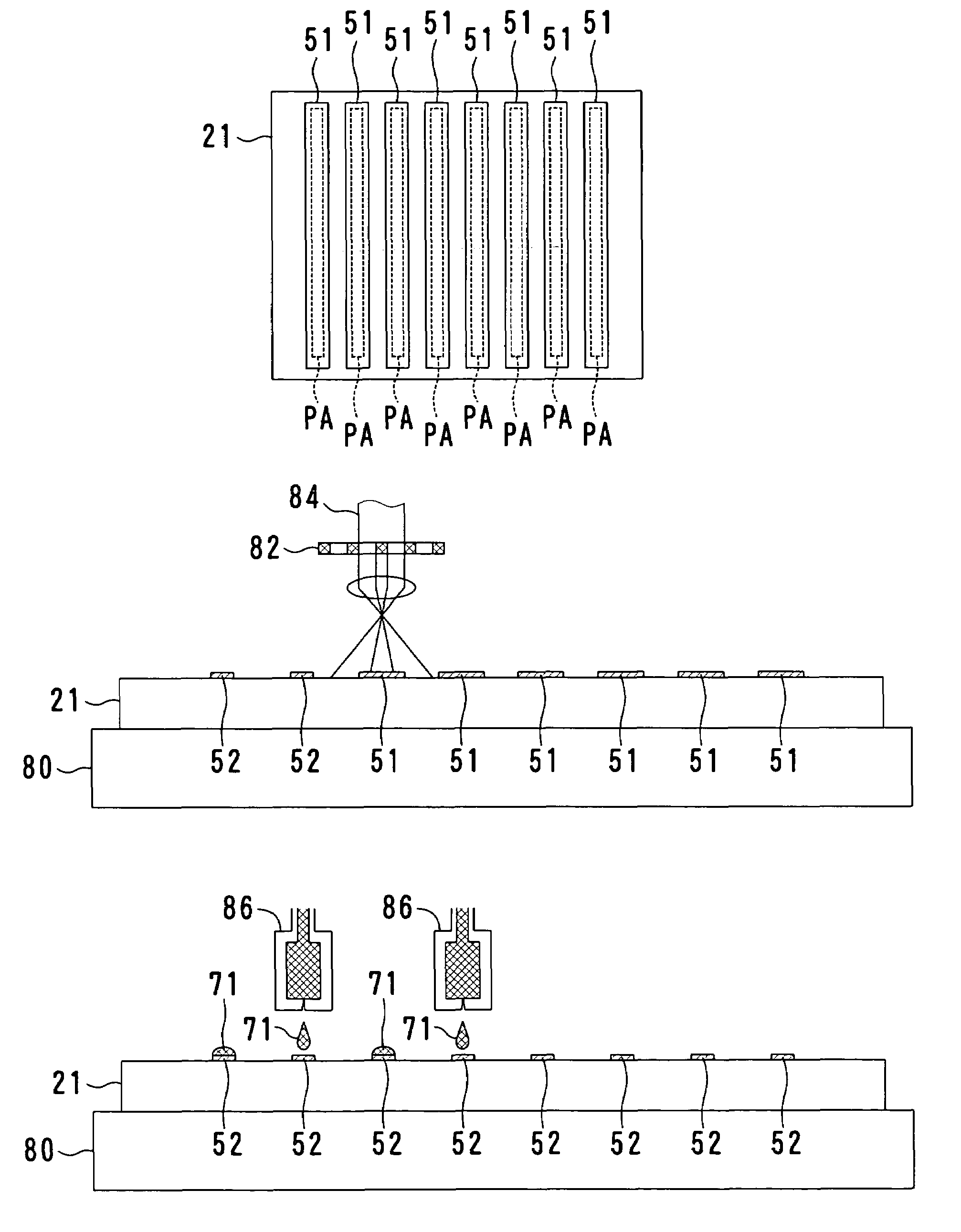
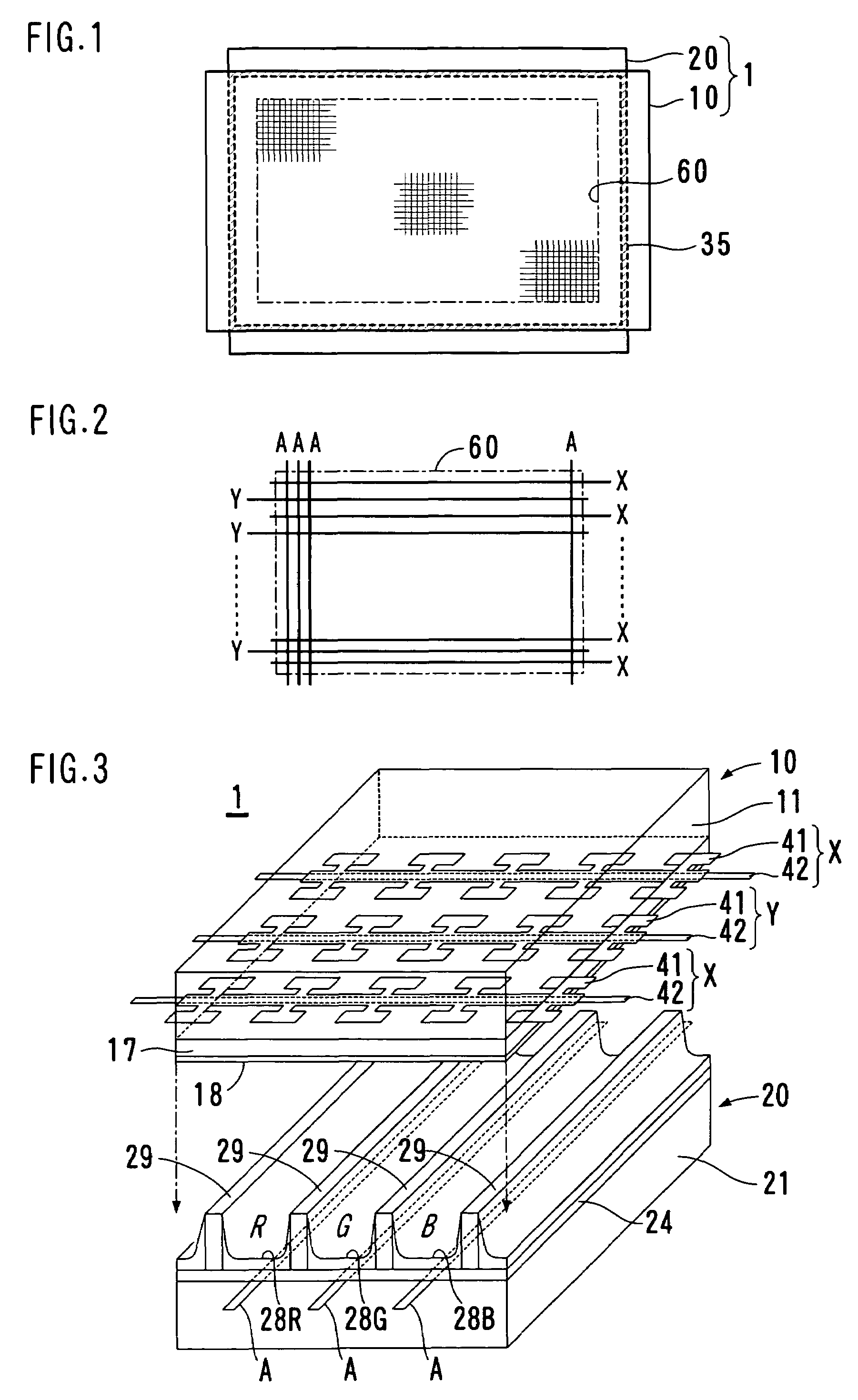
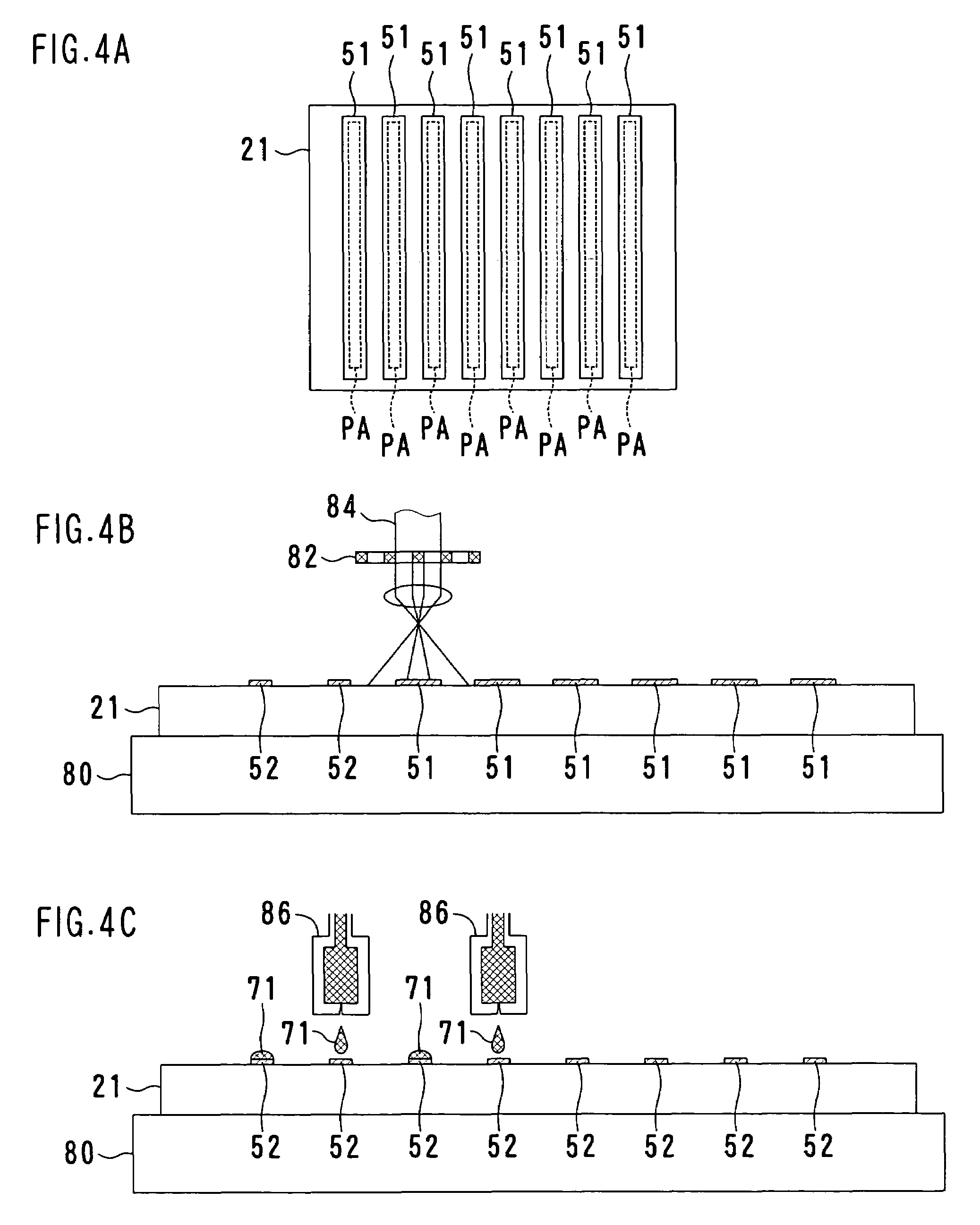
[0033]The addressing electrodes A are formed by the use of an ink jetting process in which an electroconductive inking material is jetted onto a support surface, i.e., the glass substrate 21, on which the addressing electrodes A are desired to be formed. The electroconductive inking material is in the form of a liquid medium having microparticles of silver (Ag) dispersed therein and also having a viscosity not higher than 20 mPas. Since the glass substrate 21 has no capability of absorbing and, hence, retaining deposits of the inking material on its surfaces as is well known to those skilled in the art, direct jetting of the inking material onto the glass substrate 21 would result in scattering of the jetted inking material to such an extent as to disturb formation of the desired pattern. To enable the pattern of the electrodes to be formed satisfactorily, a surface treatment is carried out to enhance the wettability of at least a surface portion of the glass substrate 21 onto which...

example 2

[0043]In place of the laser irradiation employed in the foregoing Example 1, a pattern exposure is carried out by the use of an ultraviolet lamp and a photomask to thereby accomplish the pattern shaping in which that unnecessary portion of each undercoat 51 is decomposed as hereinabove described.

example 3

[0044]In place of the formation of the ink deposits on the undercoats by the utilization of the ink jetting technique as in the foregoing Example 1, a full surface printing may be carried out with the use of a die coater to deposit the ink droplets 71 on only the undercoats 52. In such case, the electroconductive inking material is preferably of a kind difficult to deposit on the glass substrate 21, but alternatively the glass substrate 21 may be surface treated to enhance the ink repellent property prior to formation of the undercoats 52.


PUM


Abstract

To enable formation of a pattern of constituent elements, arranged in correspondence with an arrangement of cells in a display region, as desired or required with a minimized quantity of the film material, a method of manufacturing a flat panel display is provided which includes printing on a substrate a surface treating material capable of partially enhancing the wettability of the substrate, in a predetermined pattern sufficient to encompass the eventually formed pattern of constituent elements of the flat panel display. Undercoats made of the surface treating material so printed is then patterned by irradiation of light. Thereafter, utilizing the undercoats, a film material is thereafter selectively deposited on the substrate to thereby complete the predetermined pattern of the constituent elements.

Description

BACKGROUND OF THE INVENTION[0001]1. Field of the Invention[0002]The present invention relates to a method of manufacturing a flat panel display of a type having a pattern of constituent elements arranged in correspondence with an arrangement of cells in a display region.[0003]2. Description of the Prior Art[0004]In the course of mass production of flat panel displays (FPDs) such as, for example, plasma display panels, liquid crystal display panels and organic electroluminescence display panels, attempts have hitherto been made to minimize indirect materials of a kind utilized solely for the convenience of manufacture thereof. The indirect materials are, when intended products are completed, in most cases disposed of as wastes and, therefore, the need has been well recognized to minimize the indirect materials not only to avoid concomitant increase of the manufacturing cost, but also to avoid environmental contamination.[0005]The Japanese Laid-open Patent Publication No. 11-273557, p...

Claims


Application Information

Patent Timeline
Patent Type & Authority Patents(United States)
IPC IPC(8): H01J9/12G09F9/00H01J9/02H01J11/12H01J11/22H01J11/26H01J11/34
CPCH01J9/02H01J11/22H01J11/12
Inventor YAMANAKA, HIROSHI
Owner FUJITSU HITACHI PLASMA DISPLAY LTD
Why Eureka
Try Eureka