Film forming method, and film modifying method

a technology of film forming and modifying method, which is applied in the direction of transportation and packaging, nuclear engineering, railway signalling, etc., can solve the problems of high cost and largely increase and achieve the effect of increasing the growth rate of metal oxide film

Inactive Publication Date: 2006-05-02
TOKYO ELECTRON LTD
View PDF43 Cites 28 Cited by
  • Summary
  • Abstract
  • Description
  • Claims
  • Application Information

AI Technical Summary

Benefits of technology

[0010]It is the first object of the present invention to provide a film forming apparatus and method capable of increasing the growth rate of a metal oxide film.
[0011]It is the second object of the present invention to provide a film modifying apparatus and method capable of increasing the breakdown voltage of a metal oxide film in a short time.
[0012]It is the third object of the present invention to provide a film forming / modifying apparatus capable of increasing the growth rate of a metal oxide film and simultaneously increasing the breakdown voltage of the metal oxide film.

Problems solved by technology

In the film formation process, the growth rate of the tantalum oxide film is about 1 to 2 nm / min, and a great challenge is to largely increase the growth rate of the metal oxide film.
Accordingly, the throughput is insufficient to result in a high cost.

Method used


Image

  • Film forming method, and film modifying method
  • Film forming method, and film modifying method
  • Film forming method, and film modifying method

Examples


first embodiment

[0062]A film forming apparatus according to the first aspect will be described below with reference to the accompanying drawing.

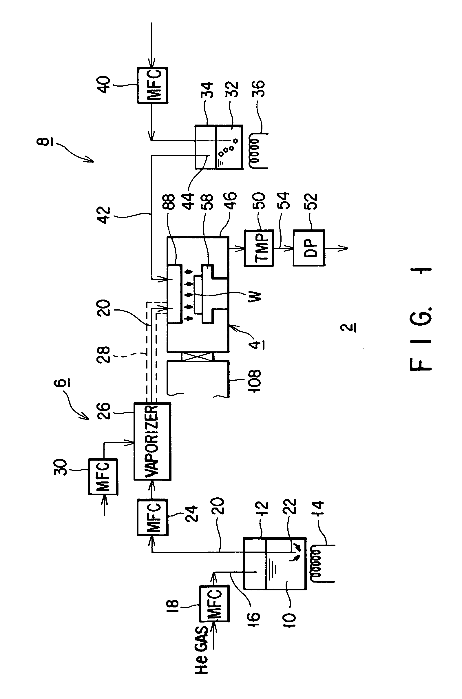
[0063]FIG. 1 is a schematic view showing the overall arrangement of the film forming apparatus according to the first embodiment of the first aspect. FIG. 2 is a view showing the main body of the film forming apparatus shown in FIG. 1. As a metal oxide film, a tantalum oxide film (Ta2O5) is formed by CVD.

[0064]A film forming apparatus 2 is mainly constituted by an apparatus main body 4, a material supply means 6 for supplying a vaporized metal oxide film material as a source gas to the apparatus main body 4, and an alcohol supply means 8.

[0065]The material supply means 6 has a closed material tank 12 which stores a liquid metal oxide film material 10, e.g., a metallic alkoxide such as Ta(OC2H5)5 as a material. The tank 12 is heated by a heater 14 to a temperature of, e.g., 20° C. to 50° C. at which the material 10 readily flows.

[0066]The distal end of a pre...

second embodiment

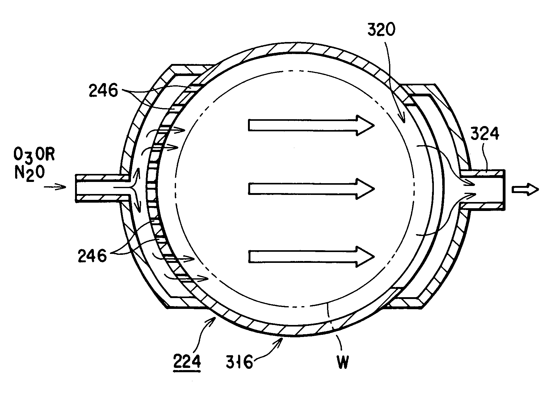
[0161]The film modifying apparatus 200B shown in FIG. 13 uses no microwave generation means, unlike the film modifying apparatus 200 shown in FIG. 9. Therefore, the structure can be simplified, and accordingly, the cost can be reduced.

[0162]In the first and second embodiments shown in FIGS. 9 and 13, the shower head 244 has a structure for supplying ozone into the disk-shaped container. However, when the pressure of ozone in the shower head 244 is relatively high, the UV ray may be absorbed in the ozone in the shower head 244 and cannot reach the wafer surface, or active oxygen atoms generated in the shower head 244 may be less likely to reach the wafer surface without vanishing.

third embodiment

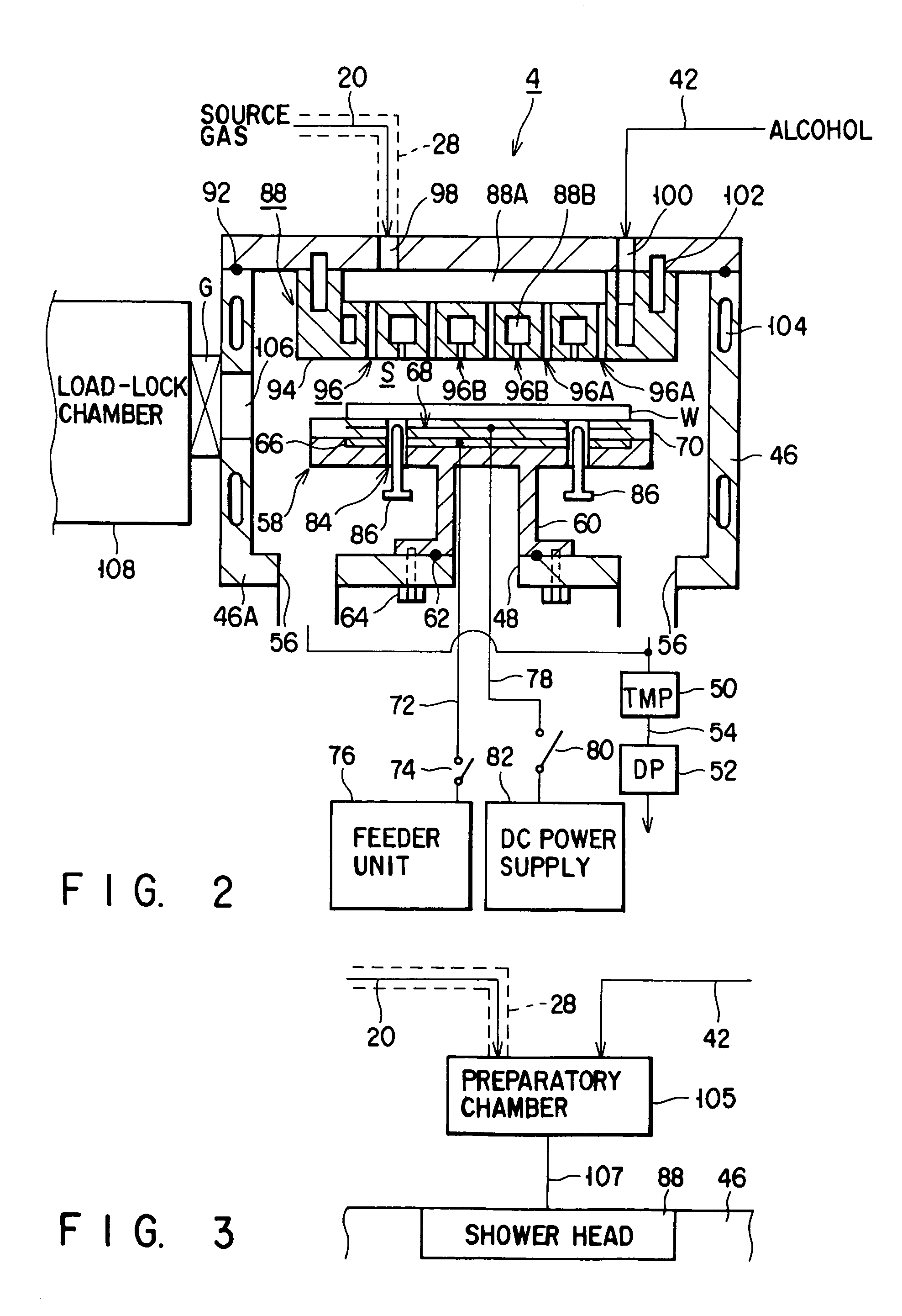
[0163]The shower head 244 may be constituted by a plurality of gas injection pipes arrayed in a matrix shape, as shown in FIGS. 14 and 15. FIG. 14 is a view showing the main part of a film modifying apparatus according to the second aspect. FIG. 15 is a bottom view showing the shower head of the film modifying apparatus shown in FIG. 14. The same reference numeral as in the above-described embodiments denote the same parts in this modification, and a detailed description thereof will be omitted. In this modification, only the main part will be described. The remaining portions have the same structures as in FIGS. 9 and 13.

[0164]As shown in FIG. 14, a film modifying apparatus 200C according to the third embodiment uses low-pressure mercury lamps as UV lamps 280. The lamps 280 are arranged above a transmission window 256. The transmission window 256 passes 90% or more of UV rays with a wavelength of, e.g., 254 nm, which are generated from the UV lamps 280.

[0165]A shower head 244 consi...


PUM

PropertyMeasurementUnit
pressureaaaaaaaaaa
temperatureaaaaaaaaaa
wavelengthaaaaaaaaaa

Abstract

A film forming and film modifying method utilizing a film forming apparatus which has an alcohol supply unit to form a metal oxide film on a semiconductor wafer in a vacuum atmosphere in which a vaporized metal oxide film material and a vaporized alcohol exist. The film modifying method irradiates a UV ray on ozone to generate active oxygen atoms, thus modifying the metal oxide film by exposing the metal oxide film to the active oxygen atoms in a vacuum atmosphere.

Description

[0001]This application is a Division of application Ser. No. 08 / 889,590 Filed on Jul. 8, 1997 now U.S. Pat. No. 6,143,081.BACKGROUND OF THE INVENTION[0002]The present invention relates to an apparatus and method of forming a metal oxide film such as a tantalum oxide film suitable for an insulating film. The present invention also relates to an apparatus and method of modifying a metal oxide film.[0003]Generally, to manufacture a semiconductor device, a semiconductor wafer is repeatedly subjected to a film formation process and a pattern etching process, thereby manufacturing a desired device. Particularly, specifications of a film forming technique are becoming stricter year by year as the density and integration of semiconductor devices become higher. For example, a very thin oxide film such as the insulating film of a capacitor or gate insulating film in a device is required to be thinner, and simultaneously, good insulating properties are required.[0004]As the insulating film, a ...

Claims


Application Information

Patent Timeline
Patent Type & Authority Patents(United States)
IPC IPC(8): B05D3/06B05D3/04C23C16/40C23C16/48C23C16/56C23C16/44C23C16/455C23C16/458C23C16/54
CPCC23C16/405C23C16/4411C23C16/45514C23C16/45563C23C16/54C23C16/45574C23C16/4586C23C16/482C23C16/45565H01L21/20
Inventor SHINRIKI, HIROSHISUGIURA, MASAHITO
Owner TOKYO ELECTRON LTD
Why Eureka
Try Eureka