Semiconductor device and manufacturing method thereof

a semiconductor and semiconductor technology, applied in semiconductor devices, semiconductor/solid-state device details, electrical apparatus, etc., can solve the problems of reduced yield, reduced mechanical strength of semiconductor elements, and increased volume of packages, and achieves high integration, low cost, and small volume

Inactive Publication Date: 2006-05-02
SEMICON ENERGY LAB CO LTD
View PDF10 Cites 72 Cited by
  • Summary
  • Abstract
  • Description
  • Claims
  • Application Information

AI Technical Summary

Benefits of technology

[0011]Based on the above problems, it is an object of the present invention to manuf

Problems solved by technology

Since the film thickness of the IC chip is comparatively thick, the lamination thereof causes increased volume of the package even if the area of the package is reduced.
However, the process is resulted to decline in mechanical strength of a semiconductor element because of leaving the polished mark of approximately 10 nm in the back surface of

Method used


Image

  • Semiconductor device and manufacturing method thereof
  • Semiconductor device and manufacturing method thereof
  • Semiconductor device and manufacturing method thereof

Examples


embodiment mode 1

[Embodiment Mode 1]

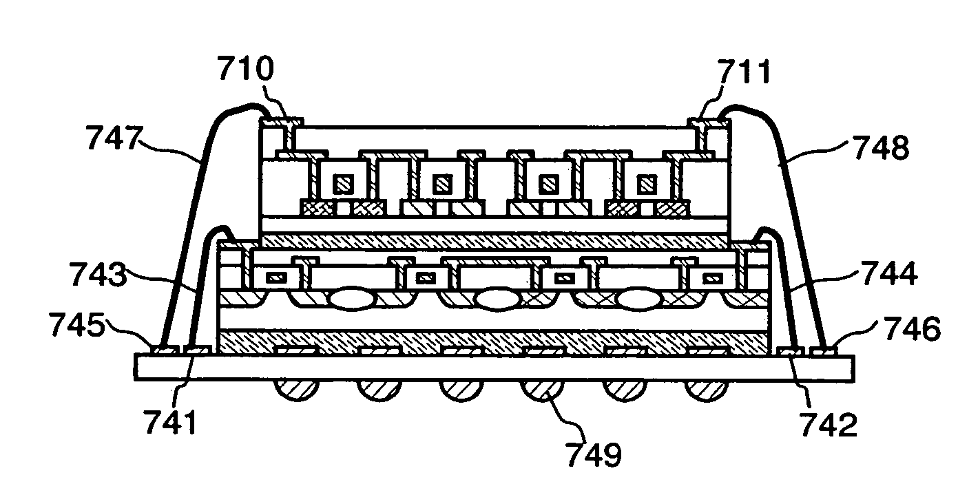
[0102]In the present embodiment mode, a semiconductor device of the present invention is described with reference to FIG. 1. FIG. 1A shows a cross sectional view of a semiconductor device in the present invention. A semiconductor element 104 in which an integrated circuit is formed by using a semiconductor substrate is provided over an insulating substrate (interposer) 101 through a wiring layer 102 and an adhesive layer 103 such as a thermo-compression bonding sheet. A semiconductor element 106 in which an integrated circuit is formed by using a semiconductor thin film is provided over the semiconductor element 104 through an adhesive layer 105 such as a thermo-compression bonding sheet. A through-hole 107 is formed in the insulating substrate, and a wiring layer 102 and an exterior terminal 108 such as a solder ball and the like are connected through the through-hole 107.

[0103]A known material such as polyimide substrate, an alumina substrate, a ceramics substra...

embodiment mode 2

[Embodiment Mode 2]

[0111]In the present embodiment mode, a method for manufacturing a semiconductor device which is shown in Embodiment Mode 1 is described. A semiconductor device of the present embodiment mode has a face up mode for all the semiconductor elements.

[0112]First, a method for manufacturing a semiconductor element (a first semiconductor element) in which an integrated circuit is formed by using a semiconductor substrate is shown in FIG. 4A. After forming a wiring portion 412 on an insulating substrate 411, the semiconductor element (the first semiconductor element) 413 in which an integrated circuit is formed by using a semiconductor substrate is bonded with an adhesive layer 414 such as a thermo-compression bonding sheet. A through-hole (107 in FIG. 1A) for connecting an exterior terminal and a semiconductor element is formed in the insulating substrate 411. The exterior terminal serves to electrically connect wirings in a mounted substrate and semiconductor elements. ...

embodiment mode 3

[Embodiment Mode 3]

[0131]In the present embodiment mode, a semiconductor device having a different structure from Embodiment Modes 1 and 2 is described. In the present embodiment mode, a point that a first semiconductor element has a flip chip mode (face down mode) is different form that of Embodiment Mode 2.

[0132]In FIGS. 5A to 5D show cross sectional views of a semiconductor device in the present embodiment mode. A wiring portion 502 over an insulating substrate 501 and an electrode pad 504 of a first semiconductor element 503 containing a semiconductor substrate are connected with a connection terminal 505 such as a bump. Note that the first semiconductor element 503, the insulating substrate 501, and the wiring portion 502 formed over the insulating substrate are fixed with a resin and the like 506. Further, the insulating substrate 501 includes a through-hole (not shown) for connecting an exterior terminal and a semiconductor element; the wiring portion 502 and the exterior ter...


PUM


Abstract

A technique for manufacturing a low-cost, small volume, and highly integrated semiconductor device is provided. A characteristic of the present invention is that a semiconductor element formed by using a semiconductor thin film is transferred over a semiconductor element formed by using a semiconductor substrate by a transfer technique in order to manufacture a semiconductor device. Compared with the conventional manufacturing method, mass production of semiconductor devices with lower cost and higher throughput can be realized, and production cost per semiconductor device can be reduced.

Description

BACKGROUND OF THE INVENTION[0001]1. Field of the Invention[0002]The present invention relates to a highly integrated semiconductor device and a manufacturing method thereof. In particular, the present invention relates to a semiconductor device on which a semiconductor element with integrated circuit (IC chip) is mounted, and a manufacturing method thereof.[0003]2. Description of the Related Art[0004]A portable electric apparatus which is represented by a cellular phone or an electronic date book is required to have various kinds of functions such as E-mail, sound recognition, image loading by a small sized camera, and Internet. Therefore, a semiconductor device (a package) having larger circuit size and larger memory volume is required.[0005]Meanwhile, a portable electric apparatus has become smaller sized, thinner, and lower cost. For this reason, a semiconductor device (package), passive components such as a resistor or the like, a mounted substrate, and the like are required to ...

Claims


Application Information

Patent Timeline
IPC IPC(8): H01L21/44H01L23/52H01L21/20H01L21/762H01L21/98H01L23/31H01L25/065
CPCH01L21/2007H01L23/3128H01L25/0657H01L25/50H01L21/76251H01L24/83H01L2924/1305H01L2221/68359H01L2221/68368H01L2224/32145H01L2224/32225H01L2224/48091H01L2224/48227H01L2224/48465H01L2224/73265H01L2225/0651H01L2225/06555H01L2924/01004H01L2924/01029H01L2924/01046H01L2924/01077H01L2924/01078H01L2924/01079H01L2924/04941H01L2924/09701H01L2924/12044H01L2924/13091H01L2924/15311H01L2924/19041H01L2924/1306H01L2924/10329H01L2924/10253H01L2924/0132H01L2224/92247H01L2224/83001H01L2224/73204H01L2224/16225H01L2224/16145H01L2924/01068H01L24/48H01L2924/00014H01L2924/00012H01L2924/00H01L2924/01031H01L2924/01033H01L2924/01042H01L2924/01074H01L24/16H01L24/73H01L2224/0401H01L2224/04042H01L2224/05624H01L2224/73253H01L2225/06517H01L2225/06558H01L2225/06568H01L2924/12042H01L2924/14H01L2924/15192H01L2924/15787H01L2924/15788H01L2924/181H01L2224/45099B81C1/00H01L23/52H01L25/07H01L27/12
Inventor KUWABARA, HIDEAKITAKAYAMA, TORUGOTO, YUUGOMARUYAMA, JUNYAOHNO, YUMIKOYAMAZAKI, SHUNPEI
Owner SEMICON ENERGY LAB CO LTD
Why Eureka
Try Eureka