Integrated circuit memory architecture with selectively offset data and address delays to minimize skew and provide synchronization of signals at the input/output section

a technology of integrated circuits and memory architectures, applied in the field of integrated circuit devices, to minimize skew and provide synchronization of signals at the input/output section, and achieve the effect of minimizing skew

Active Publication Date: 2006-05-02
PROMOS TECH INC
View PDF3 Cites 11 Cited by
  • Summary
  • Abstract
  • Description
  • Claims
  • Application Information

AI Technical Summary

Benefits of technology

[0012]Also further disclosed herein is a technique for minimizing skew between clock and data signals at a data output block of an integrated circuit memory device comprising a plurality of memory arrays. The technique comprises selectively adding delays to address and clock information buses coupled to the memory arrays such that a cumulative delay to signals generated on the address and clock information buses increases as a position of each of the memory arrays becomes more distal from an address / clock generation block and selectively adding delays to a data bus coupled to the memory arrays such that a cumulative delay to signals output on the data bus decreases as a position of each of the memory arrays becomes more proximate to the data output block such that a total delay added to the address, clock information and data buses for each of the memory arrays is substantially constant.

Problems solved by technology

However, with extremely large chips, two extreme cases result.
Secondly, sub-arrays more remote from the address / control section receive those signals relatively slowly while the “read” data is only a short delay from the device I / O section.

Method used


Image

  • Integrated circuit memory architecture with selectively offset data and address delays to minimize skew and provide synchronization of signals at the input/output section
  • Integrated circuit memory architecture with selectively offset data and address delays to minimize skew and provide synchronization of signals at the input/output section
  • Integrated circuit memory architecture with selectively offset data and address delays to minimize skew and provide synchronization of signals at the input/output section

Examples


Embodiment Construction

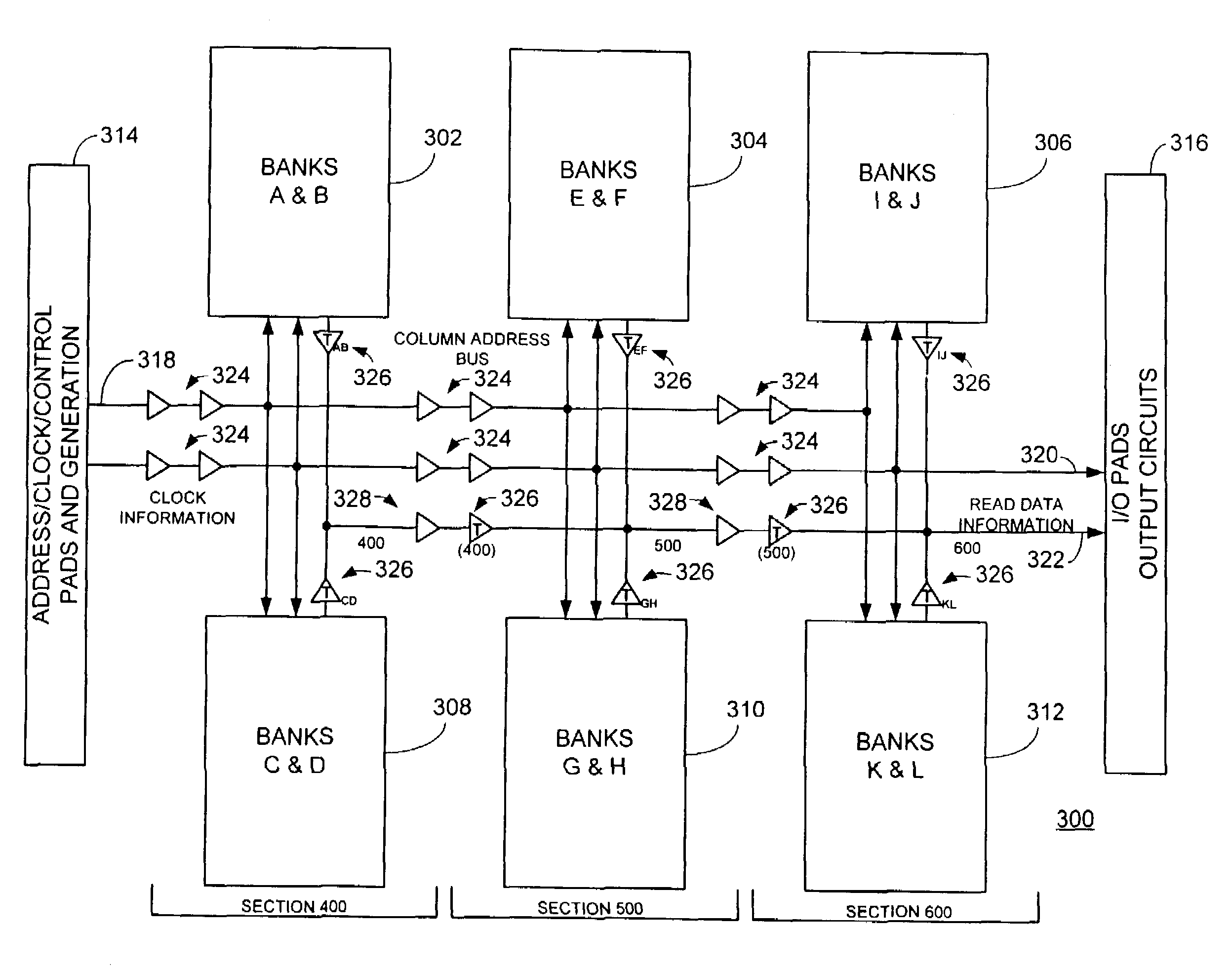
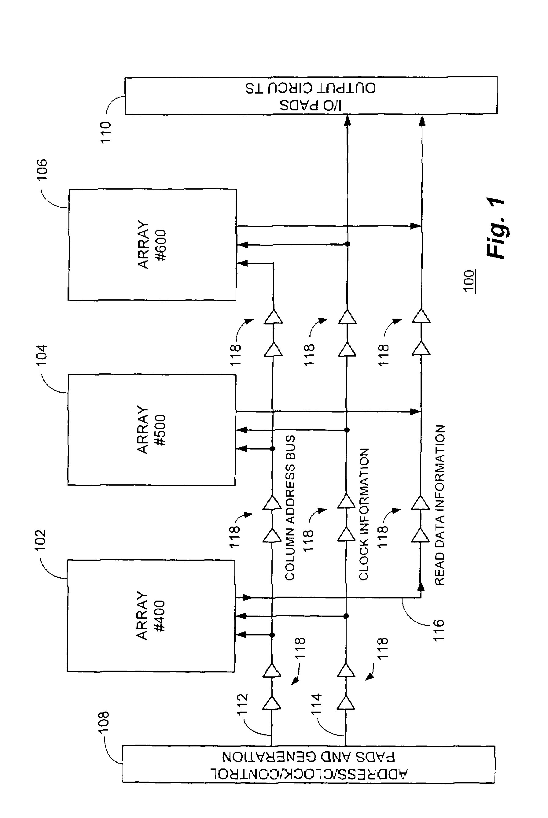
[0017]With reference now to FIG. 1, a simplified functional block diagram of a representative embodiment of an integrated circuit memory device 100 architecture is shown incorporating offset data and address delays in accordance with the present invention. A number of memory arrays 102, 104 and 106 comprising, for example, SDRAM are illustrated as Array #400, Array #500 and Array #600 respectively.

[0018]An address / clock / control pads and generation block 108 provides column address information on a column address bus 112 and clock information on a clock address bus 114 to the various memory arrays 102, 104 and 106 as well as to the memory device 100 input / output (“I / O”) pads and output circuit block 110. Each of the memory arrays 102, 104 and 106 provides data read out of the memory cells to a read data information bus 116 which is also supplied to the I / O pads and output circuit block 110. In accordance with the present invention, a first group of driver pairs 118 are interposed on ...


PUM


Abstract

An integrated circuit memory architecture with selectively offset data and address delays to minimize skew and provide synchronization of signals at the input/output section in which the architecture is divided into memory sections, depending upon their distance from the address/control generation block. The address and clock information is re-driven between these sections, which effectively serves to add a quantized number of gate delays in the address path between the sections while concomitantly minimizing skew. A corresponding number of gate delays is also added to the “read” data path for each section such that the number of delays in the address/clock path plus the number of delays in the “read” data path is substantially constant.

Description

BACKGROUND OF THE INVENTION[0001]The present invention relates, in general, to the field of integrated circuit (“IC”) devices incorporating memory arrays. More particularly, the present invention relates to an integrated circuit memory architecture with selectively offset data and address delays to minimize skew and provide synchronization of signals at the input / output section.[0002]Many types of DRAM based devices, or integrated circuits including embedded memory arrays, are currently available including extended data out (“EDO”), synchronous DRAM (“SDRAM”), double data rate (“DDR”) DRAM and the like. Regardless of configuration, the primary purpose of the DRAM is to store data. Functionally, data may be written to the memory, read from it or periodically refreshed to maintain the integrity of the stored data. In current high density designs, each DRAM memory cell comprises a single pass transistor coupled to an associated capacitor that may be charged to store a value representat...

Claims


Application Information

Patent Timeline
Patent Type & Authority Patents(United States)
IPC IPC(8): G06F13/42H04L7/00G06F17/50G11C7/10G11C11/408G11C11/4097
CPCG06F17/505G11C11/4097G11C7/222G11C11/4085G11C7/10G06F2217/62G06F30/327G06F30/396
Inventor FAUE, JON ALLANMEADOWS, HAROLD BRETT
Owner PROMOS TECH INC
Why Eureka
Try Eureka