SONOS structure including a deuterated oxide-silicon interface and method for making the same

a deuterated oxide and silicon interface technology, applied in the field of semiconductor/solid-state device manufacturing, can solve the problems of affecting the efficiency of semiconductor fabrication processes, affecting the efficiency of semiconductor manufacturing, so as to reduce the safety hazards of semiconductor fabrication processes, improve the durability and retention of devices fabricated by the method described herein, and increase the thermal budget of devices.

Inactive Publication Date: 2006-05-09
LONGITUDE FLASH MEMORY SOLUTIONS LTD
View PDF6 Cites 43 Cited by
  • Summary
  • Abstract
  • Description
  • Claims
  • Application Information

AI Technical Summary

Benefits of technology

[0015]There may be several advantages to processing a semiconductor topography according to the method described herein. For example, deuterium may be diffused across an oxide-silicon interface such that dangling bonds within the interface may be passivated. In this manner, the endurance and retention of devices fabricated by the method described herein may be improved. In addition, dangling bonds of devices including nitride layers, such as SONOS devi

Problems solved by technology

Sometimes, however, irregularities may exist within the silicon surface or may be created during the formation of the oxide layer, both of which may bring about a disjointed oxide pattern which can lead to dangling bonds, often referred to as “interface traps” at the oxide-silicon interface.
Consequently, interface traps may cause a variety of problems, such as shifts in the threshold voltage (Vt) of an ensuing device and/or breakdown of the oxide layer.
In addition, the build-up of mobile carriers may increase the back tunneling current of non-volatile semiconductor memory cells, thereby dissipating the memory of the cells more quickly.
Consequently, the presence of interface traps may degrade the long-term retention of non-volatile memory cells.
Although using hydrogen or deuterium anneals may passivate interface traps of fabricated devices, using such anneals may present problems affecting the functionality and reliability of the devices.
Typically, free hydrog

Method used


Image

  • SONOS structure including a deuterated oxide-silicon interface and method for making the same
  • SONOS structure including a deuterated oxide-silicon interface and method for making the same
  • SONOS structure including a deuterated oxide-silicon interface and method for making the same

Examples


Embodiment Construction

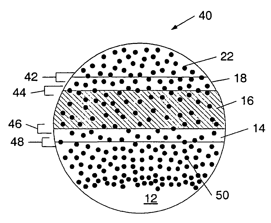
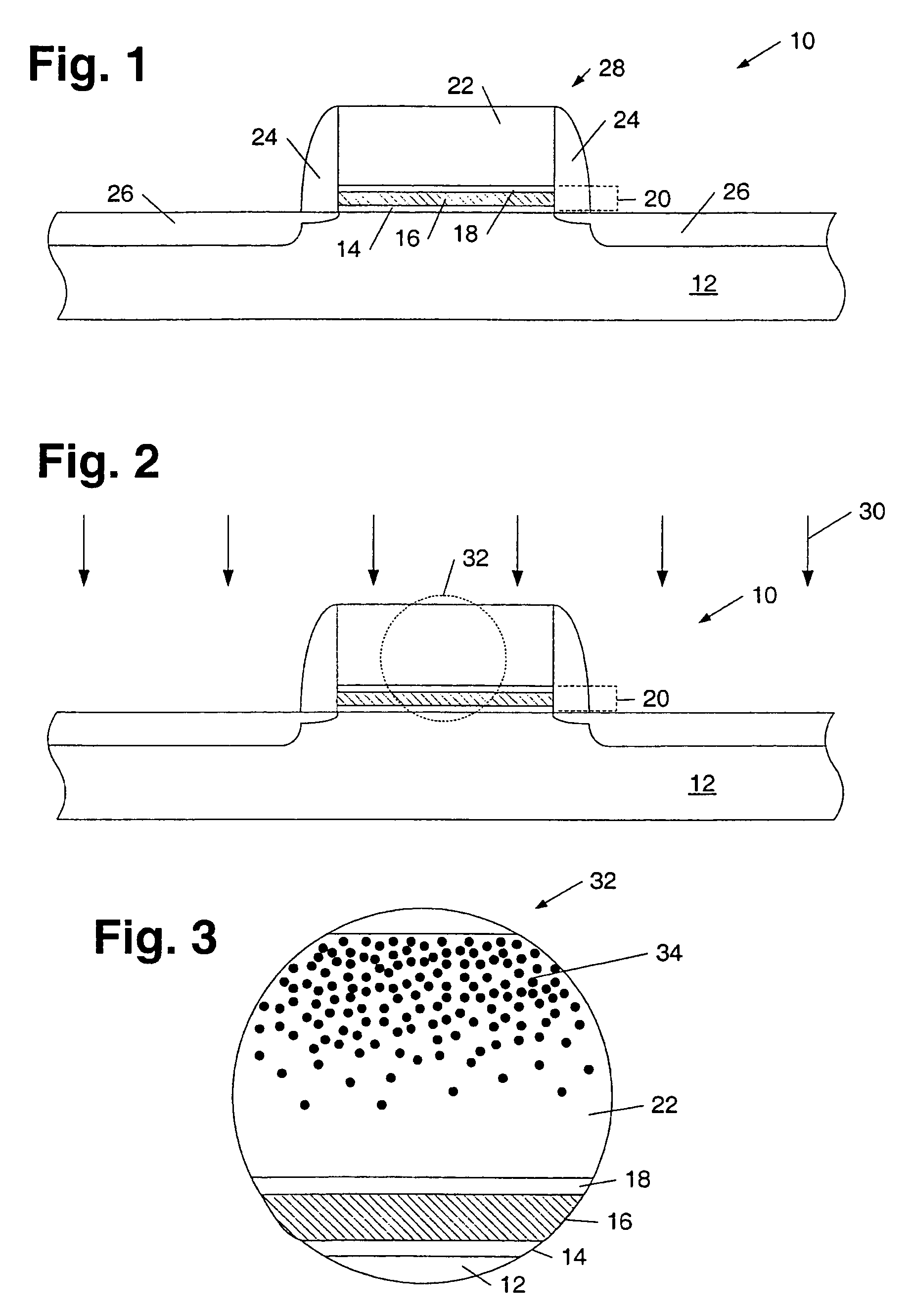
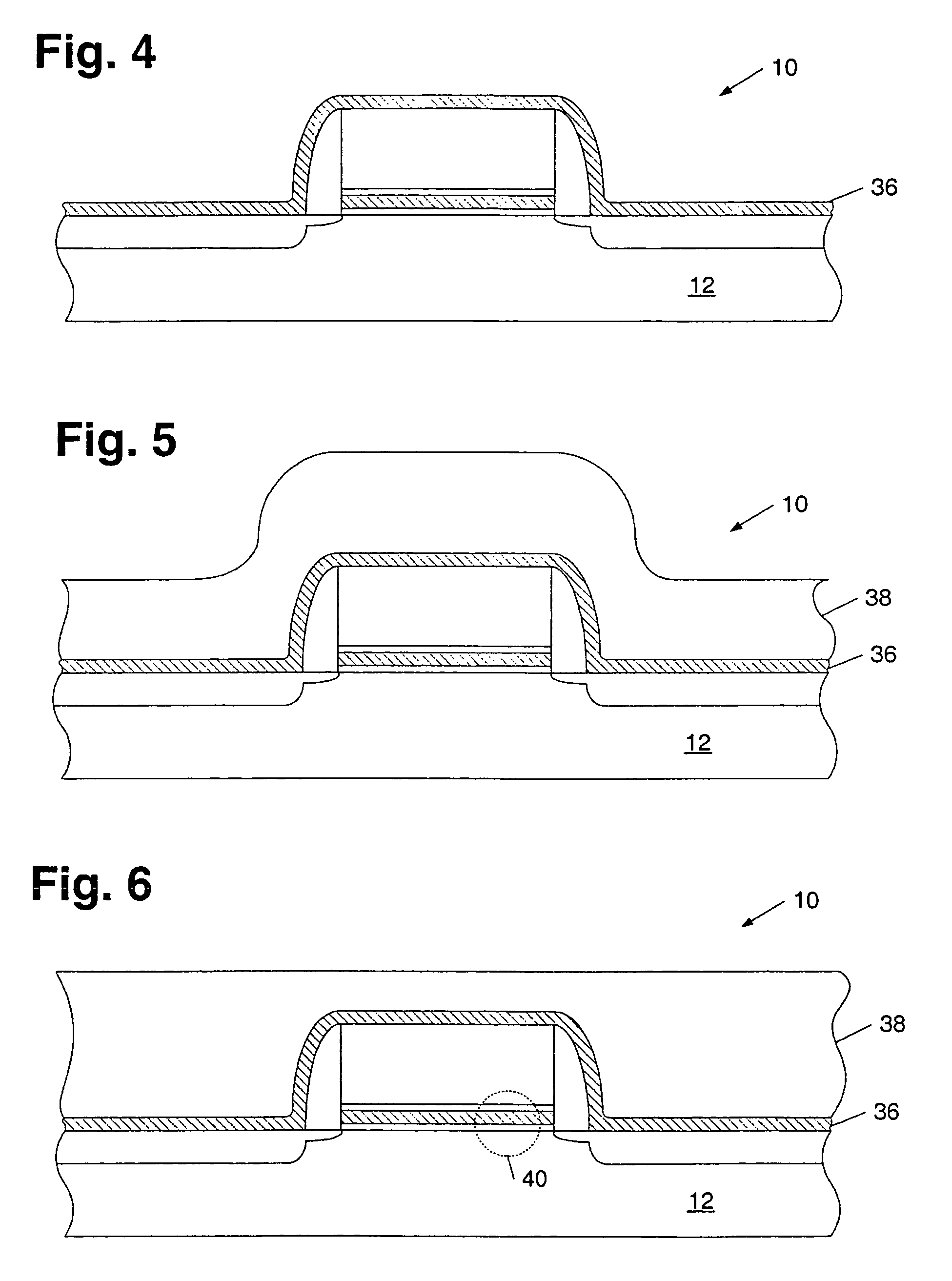
[0026]Turning to the drawings, exemplary embodiments of a method for processing a semiconductor topography are shown in FIGS. 1–8. In particular, exemplary embodiments of a method for diffusing deuterium across one or more interface layers of a silicon-oxide-nitride-oxide-silicon (SONOS) structure during a reflow process of a dielectric layer spaced above the SONOS structure is provided. FIG. 1 depicts a partial cross-sectional view of semiconductor topography 10 with SONOS structure 28 arranged upon semiconductor layer 12. Semiconductor layer 12 may be a silicon-based semiconductor substrate such as a monocrystalline silicon, silicon-germanium, silicon-on-insulator, or silicon-on-sapphire substrate. In addition, semiconductor layer 12 may be doped either n-type or p-type. Alternatively, semiconductor layer 12 may be substantially undoped. In yet other embodiments, semiconductor layer 12 may include structures and layers formed upon a semiconductor substrate. The structures and laye...


PUM


Abstract

A method for processing a semiconductor topography is provided, which includes diffusing deuterium across one or more interfaces of a silicon-oxide-nitride-oxide-silicon (SONOS) structure. In particular, the method may include diffusing deuterium across one or more interfaces of a SONOS structure during a reflow of a dielectric layer spaced above the SONOS structure. In some embodiments, the method may include forming a deutereated nitride layer above the SONOS structure prior to the reflow process. In addition or alternatively, the method may include forming a deutereated nitride layer within the SONOS structure prior to the reflow process. In some cases, the method may further include annealing the SONOS structure with a deutereated substance prior to forming the deutereated nitride layer. In either embodiment, a SONOS structure may be formed which includes deuterium arranged within an interface of a silicon layer and an oxide layer of the structure.

Description

[0001]This application is a divisional application from prior application SN 10 / 094,108 filed Mar. 8, 2002, now U.S. Pat. No. 6,677,213.BACKGROUND OF THE INVENTION[0002]1. Field of the Invention[0003]This invention relates to semiconductor device manufacturing, and more particularly, to an improved oxide-nitride layer and a method for making the same.[0004]2. Description of the Related Art[0005]The following descriptions and examples are not admitted to be prior art by virtue of their inclusion within this section.[0006]The formation of oxide layers upon silicon layers is commonly used within fabrication processes of a variety of semiconductor devices. Sometimes, however, irregularities may exist within the silicon surface or may be created during the formation of the oxide layer, both of which may bring about a disjointed oxide pattern which can lead to dangling bonds, often referred to as “interface traps” at the oxide-silicon interface. Dangling bonds are generally sporadic silic...

Claims


Application Information

Patent Timeline
IPC IPC(8): H01L29/76H01L29/94H01L31/062H01L31/113H01L31/119H01L21/28H01L21/30H01L29/51H01L29/792
CPCH01L21/28176H01L21/28194H01L21/28202H01L29/792H01L21/3003H01L29/513H01L29/518H01L21/28282H01L29/40117
Inventor RAMKUMAR, KRISHNASWAMYJENNE, FREDERICK B.
Owner LONGITUDE FLASH MEMORY SOLUTIONS LTD
Why Eureka
Try Eureka