Method for preparing ferroelectric thin film through magnetron sputtering and ferroelectric thin film

A ferroelectric thin film and magnetron sputtering technology, applied in sputtering plating, ion implantation plating, metal material coating process, etc., can solve the problem of increasing device thermal budget, reducing process efficiency, and damage to device structure and performance, etc. problem, achieve the effect of high residual polarization intensity, solve excessive requirements, and prevent thermal budget

Inactive Publication Date: 2019-02-19
XIANGTAN UNIV
View PDF2 Cites 6 Cited by
  • Summary
  • Abstract
  • Description
  • Claims
  • Application Information

AI Technical Summary

Problems solved by technology

However, no matter which technology is used, there are certain defects. For example, double-target sputtering has high requirements for equipment, which increases the process threshold for thin film preparation, and high-temperature sputtering reduces the efficiency of the process.
However, single target sputtering needs to be sputtered at high temperature, which requires high temperature, and the high temperature requirement increases the thermal budget of the device, which will damage the structural performance of the device prepared by the previous process.

Method used


Image

  • Method for preparing ferroelectric thin film through magnetron sputtering and ferroelectric thin film
  • Method for preparing ferroelectric thin film through magnetron sputtering and ferroelectric thin film
  • Method for preparing ferroelectric thin film through magnetron sputtering and ferroelectric thin film

Examples


Embodiment 1

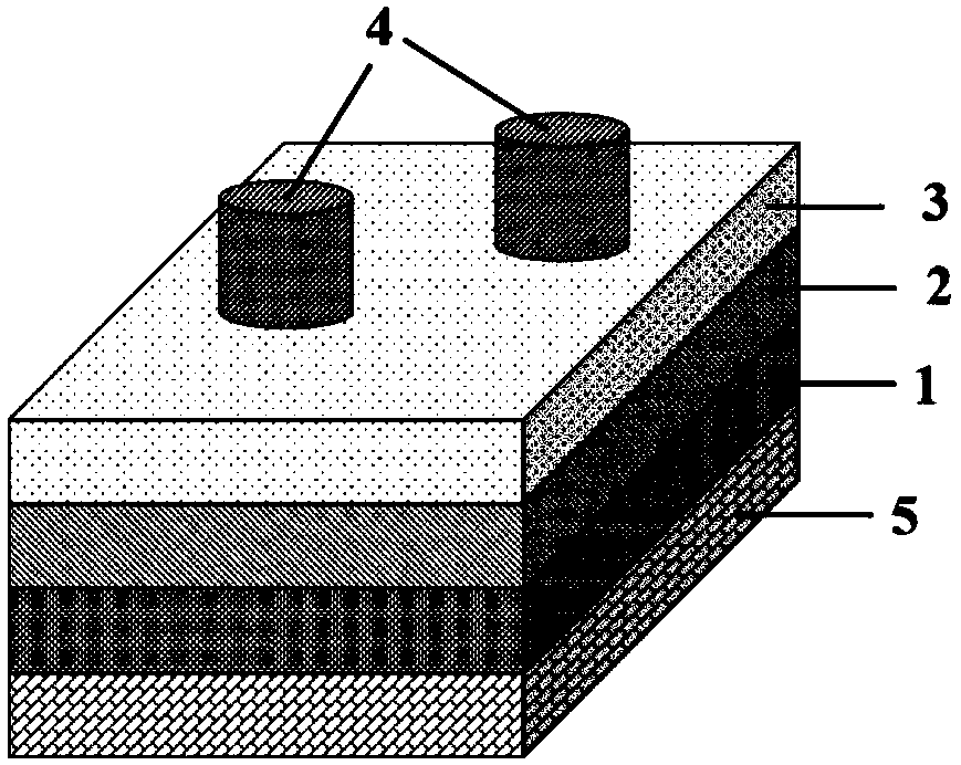
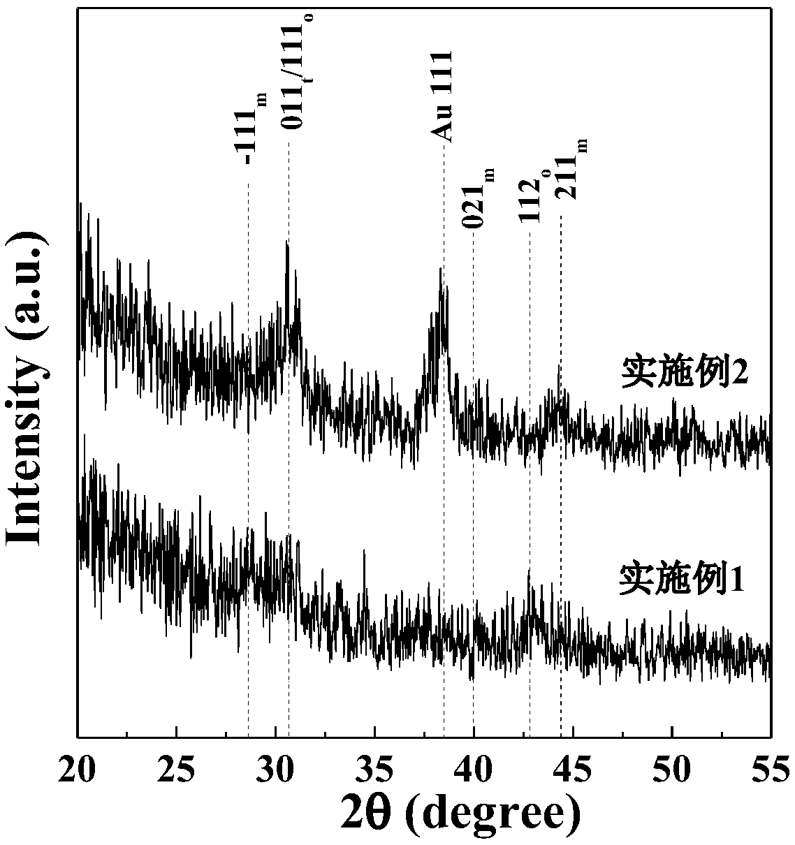
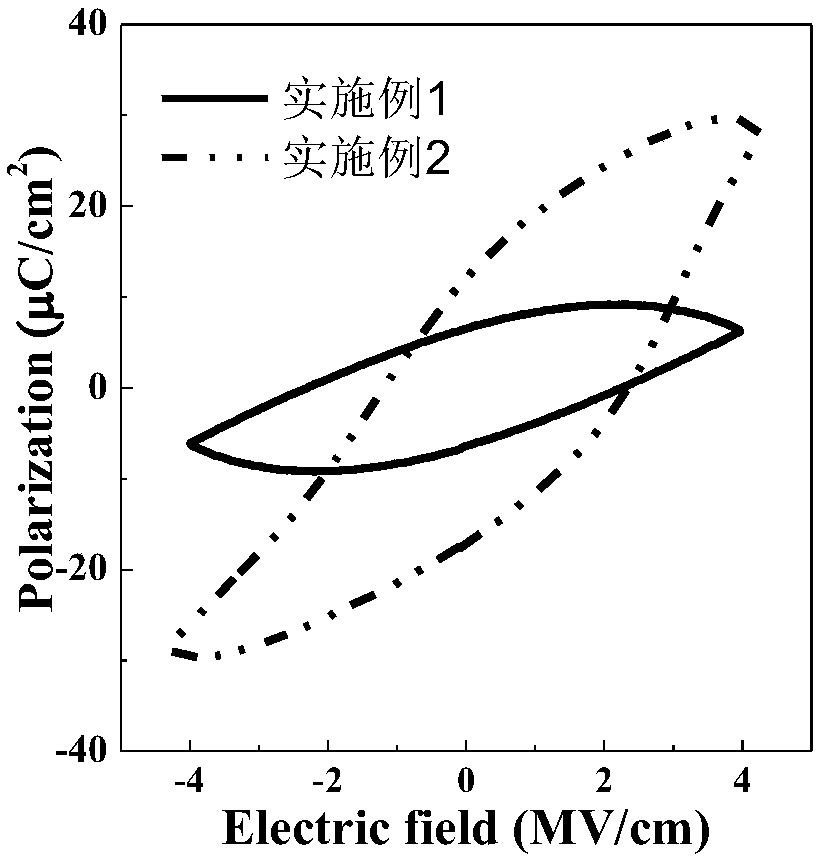
[0089] Will n + -Si(100) substrate with 98% H 2 SO 4 With 30% H 2 O 2 The mixing ratio is 5:5 solution cleaning for 10 minutes to remove surface organic matter and particles. After rinsing with deionized water, soak in 1% HF solution for 8s to remove the silicon surface oxide layer. Will clean n + -Si (100) substrate and zirconium-doped hafnium oxide-based ceramic target are placed in the reaction chamber. Adjust the vacuum degree of the reaction chamber, first use a mechanical pump to vacuum the reaction chamber to 10 -2 Pa, then use mechanical pump and molecular pump to simultaneously evacuate the reaction chamber to 10 -5 Pa; Then pass argon and oxygen with a flow ratio of 10:1 into the reaction chamber to adjust the pressure of the reaction chamber to 2Pa and adjust the power to 60W. Under this pressure and power condition, the ignited plasma source ionizes the introduced gas to form an ion current. The ion current is used to bombard the surface of the zirconium-doped hafni...

Embodiment 2

[0092] Will n + -Si(100) substrate with 98% H 2 SO 4 With 30% H 2 O 2 The mixture ratio is 1:1 solution for cleaning for 10 minutes to remove surface organic matter and particles. After rinsing with deionized water, soak in 1% HF solution for 10s to remove the silicon surface oxide layer. Will clean n + -Si(100) substrate and zirconium-doped hafnium oxide-based ceramic target are placed in the reaction chamber, and the zirconium-doped hafnium oxide-based ceramic target is adjusted to n + -Si (100) substrate distance to 55mm. Adjust the vacuum degree of the reaction chamber, first use a mechanical pump to vacuum the reaction chamber to 10 -2 Pa, then use mechanical pump and molecular pump to simultaneously evacuate the reaction chamber to 10 -6 Pa; then pass pure argon into the reaction chamber to adjust the pressure of the reaction chamber to 2Pa and adjust the power to 60W. Under this pressure and power condition, the ignited plasma source ionizes the introduced gas to form an ...

Embodiment 3

[0095] Will n + -Si(100) substrate with 98% H 2 SO 4 With 30% H 2 O 2 The mixed solution is cleaned for 10 minutes to remove surface organic matter and particles. After rinsing with deionized water, it is soaked in 1% HF solution for 10s to remove the silicon surface oxide layer. Will clean n + -Si(100) substrate is placed in the reaction chamber to adjust the zirconium-doped hafnium oxide-based ceramic target and n + -Si (100) substrate distance to 55mm. Adjust the vacuum degree of the reaction chamber, first use a mechanical pump to vacuum the reaction chamber to 10 -2 Pa, then use mechanical pump and molecular pump to simultaneously evacuate the reaction chamber to 10 -6 Pa; then pass pure argon into the reaction chamber to adjust the pressure of the reaction chamber to 2Pa and adjust the power to 50W. Under this pressure and power condition, the ignited plasma source ionizes the introduced gas to form an ion current. The ion current is used to bombard the surface of the zir...


PUM

PropertyMeasurementUnit
thicknessaaaaaaaaaa
thicknessaaaaaaaaaa
thicknessaaaaaaaaaa

Abstract

The invention discloses a method for preparing a ferroelectric thin film through magnetron sputtering. The method comprises the following steps that S1, a single sputtering target material and a substrate are arranged in a reaction chamber; S2, sputtering is carried out on the target material at the room temperature so as to obtain atoms and or an atomic group; S3, the atoms and/or the atom groupbetween the target material and the substrate under the action of an electric field and a magnetic field is deposited on the substrate to obtain a pre-formed ferroelectric thin film; and S4, annealingtreatment is carried out on the pre-formed ferroelectric thin film to obtain the ferroelectric thin film. According to the method for preparing the ferroelectric thin film through magnetron sputtering, the single sputtering target material is arranged in the reaction chamber, sputtering is carried out at room temperature, and magnetron deposition is carried out to prepare the ferroelectric thin film, so that the problems that the temperature requirement is excessively high during single-target sputtering in the prior art, and the requirement for an instrument during double-target sputtering is strict are solved.

Description

Technical field [0001] The invention relates to the technical field of thin film material preparation, in particular to a method for preparing a ferroelectric thin film by magnetron sputtering and a ferroelectric thin film. Background technique [0002] Ferroelectric thin film is the core material of ferroelectric memory, and its performance and preparation process determine the cost and performance reliability of its integrated devices. The traditional hafnium oxide film and its doped series have been widely used as gate dielectric materials in metal-oxide-silicon field effect transistors (MOSFETs), which are extremely strong with complementary metal-oxide-silicon (CMOS) processes. Process compatibility. On the one hand, the breakdown electric field, residual polarization strength, coercive electric field and other properties of the hafnium oxide film can be comparable or even better than the traditional perovskite ferroelectric film. On the other hand, the preparation process ...

Claims


Application Information

Patent Timeline
Patent Type & Authority Applications(China)
IPC IPC(8): C23C14/06C23C14/08C23C14/35C23C14/58
CPCC23C14/0688C23C14/083C23C14/35C23C14/5806
Inventor 廖佳佳周益春廖敏姜杰曾斌建彭强祥
Owner XIANGTAN UNIV
Why Eureka
Try Eureka