Direct attachment of semiconductor chip to organic substrate

a technology of organic substrates and semiconductor chips, applied in the direction of semiconductor devices, semiconductor/solid-state device details, electrical equipment, etc., can solve the problems of high cost of plasma treatment, high cost of both metal layers and adhesive layers, and the inability to maximize adhesion, etc., to achieve the effect of reducing the cost of molding compounds and methods

Inactive Publication Date: 2006-05-09
TEXAS INSTR INC
View PDF14 Cites 8 Cited by
  • Summary
  • Abstract
  • Description
  • Claims
  • Application Information

AI Technical Summary

Benefits of technology

[0023]In yet another aspect of the invention, benefits are derived from the fast-speed singulation methods (such as sawing) of the asse

Problems solved by technology

Progress has been made in reducing the area and height requirements of packages, but frustrating problems still remain in maximizing adhesion, device reliability assurance and manufacturing cost reduction.
Unfortunately, the process of using both and a metal layer and an adhesive layer is expensive.
Furthermore, the authors found that the plasma treatment increases the polyimide surface roughness.
From the standpoint of cos

Method used


Image

  • Direct attachment of semiconductor chip to organic substrate
  • Direct attachment of semiconductor chip to organic substrate
  • Direct attachment of semiconductor chip to organic substrate

Examples


Embodiment Construction

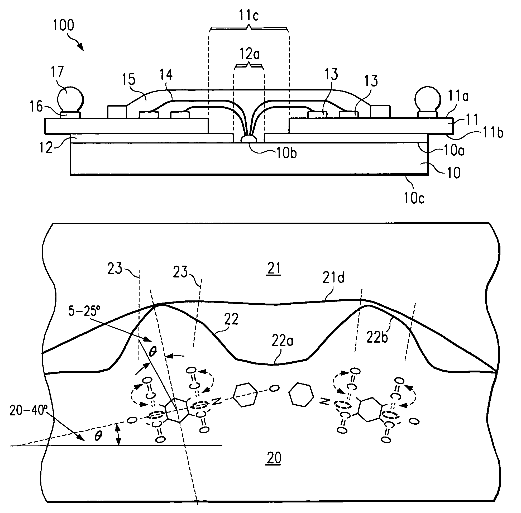
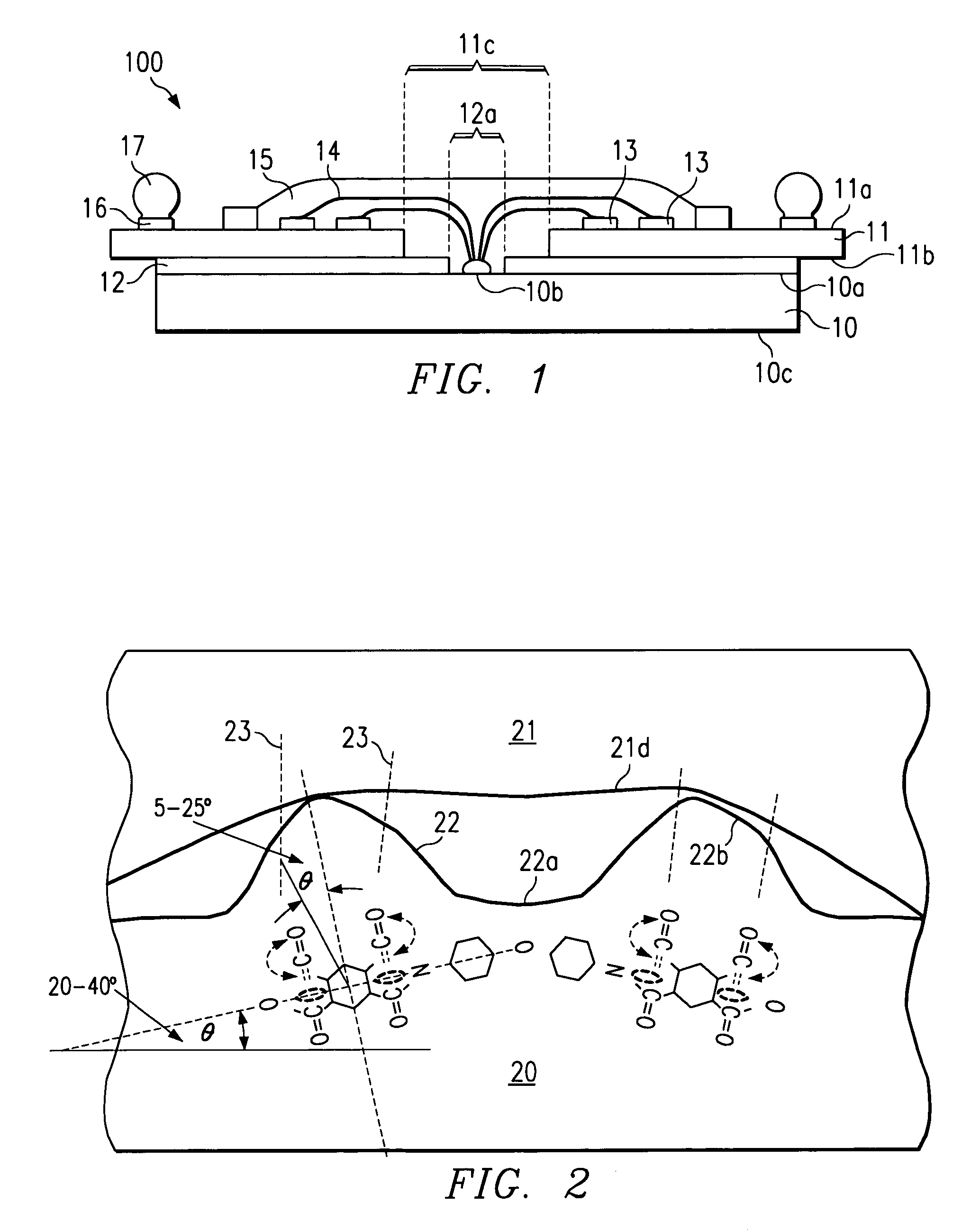
[0030]The present invention is related to high frequency, high speed integrated circuit (IC) packages having both a low profile and a small outline. As defined herein, the term “outline” relates to the overall width and length of, for example, the entire IC package. The outline of the IC package is also referred to as the footprint of the IC package, because it defines the surface area on a motherboard that the IC package will occupy. Outline will be measured in, for example, square millimeters. As defined herein, the term “profile” refers Lo thickness or height of, for example, the IC package. The profile will be measured in, for example, millimeters. As defined herein, the term “substantially the same” refers to the relative outlines of the substrate and the semiconductor chip, which are within less than about 10% of one another. In embodiments where the chip and the substrate have the same outlines, the package is referred to as chip-size package. Importantly, the term substantia...


PUM


Abstract

A method for attaching an integrated circuit chip to an organic substrate comprising the steps of providing an integrated circuit chip having an active and a passive surface, said active surface including a protective polymer layer; activating said polymer layer by exposing it to reactive ion etching plasma, thereby increasing the surface roughness and imparting affinity to adhesion; providing an electrically insulating substrate having first and second surfaces; and contacting said second surface of said substrate to said activated polymer layer on said chip, whereby strong adhesion is exerted at the interface between said layer and said substrate, directly attaching said substrate to said chip.

Description

[0001]This is a divisional application of Ser. No. 09 / 401,572, filed Sep. 22, 1999, U.S. Pat. No. 6,602,803.[0002]The present invention is related in general to the field of semiconductor devices and processes, and more specifically to methods for reliably assembling integrated circuit chips directly onto organic substrates.BACKGROUND OF THE INVENTION[0003]One of the major trends in semiconductor packaging is the effort to shrink the package outline so that the package consumes less area and less height when it is mounted onto the circuit board. Another powerful trend is the effort to achieve the outline reduction with minimum cost (both material and manufacturing cost). One of the most successful approaches has been the development of so-called “chip-scale packages”. These packages have an outline adding less than 20% to the chip area. A chip-scale package which has only the size of the chip itself, is often referred to as “chip-size package”.[0004]Within the semiconductor memory p...

Claims


Application Information

Patent Timeline
IPC IPC(8): H01L23/495H01L23/31
CPCH01L23/3114H01L24/49H01L23/3142H01L2924/10253H01L24/45H01L2224/45144H01L2224/48091H01L2224/48095H01L2224/48227H01L2224/4824H01L2224/48465H01L2224/49H01L2224/73215H01L2924/01002H01L2924/01005H01L2924/01006H01L2924/01013H01L2924/01014H01L2924/01028H01L2924/01029H01L2924/01031H01L2924/01032H01L2924/01039H01L2924/01047H01L2924/01049H01L2924/0105H01L2924/01078H01L2924/01079H01L2924/01082H01L2924/014H01L2924/12044H01L2924/14H01L2924/1433H01L2924/15311H01L2924/20105H01L2924/20106H01L2224/32225H01L2924/01033H01L2924/01087H01L24/48H01L2924/00014H01L2924/00H01L2224/06135H01L2224/06136H01L2924/181
Inventor YEW, CHEE KIANGAMAGAI, MASAZUMI
Owner TEXAS INSTR INC
Why Eureka
Try Eureka