Soft defect printability simulation and analysis for masks

a mask and printability technology, applied in the field of integrated circuit manufacturing, can solve the problems of masks that are either initially or after repair, can not automatically identify soft defects, much less determine the impact of soft defects, etc., and achieve the effect of improving the computed transmission of these images

Active Publication Date: 2006-05-09
SYNOPSYS INC
View PDF35 Cites 41 Cited by
  • Summary
  • Abstract
  • Description
  • Claims
  • Application Information

AI Technical Summary

Benefits of technology

[0019]At this point, a transmission, a phase, and a shape for both the host image and the defect image can be computed. Note that the defect and host images are analyzed separately because their respective transmission and phase information are obtained using different processes. However, once this information is obtained, the defect and host images can be combined to generate a corrected test image. Transmission, phase, and shape information can also be computed for the reference image, thereby generating a corrected reference image. Using the corrected test image and the corrected reference image, a simulated test wafer image based on the corrected test image and a simulated reference wafer image based on the corrected reference image can be generated. In one embodiment, a trim mask image can be used in generating the simulated test wafer image and the simulated reference wafer image, thereby simulating the second exposure in double exposure phase shifting mask technology. In general, a supplemental mask image can be used in generating the simulated test wafer image and the simulated reference wafer image, thereby simulating another exposure in a multiple exposure phase shifting mask technology. In another embodiment, because the stepper (i.e. the tool transferring the mask pattern to the wafer) and the inspection tool (i.e. the tool generating the test image) may have different optical settings, the transmission and the phase of the defect, host, and reference images can be calibrated, thereby improving the computed transmission for these images.

Problems solved by technology

These masks, either initially or after repair, can have “soft” defects, e.g. phase and / or transmission defects.
Unfortunately, tools currently used in the industry cannot automatically identify, much less determine the impact of these soft defects.

Method used


Image

  • Soft defect printability simulation and analysis for masks
  • Soft defect printability simulation and analysis for masks
  • Soft defect printability simulation and analysis for masks

Examples


Embodiment Construction

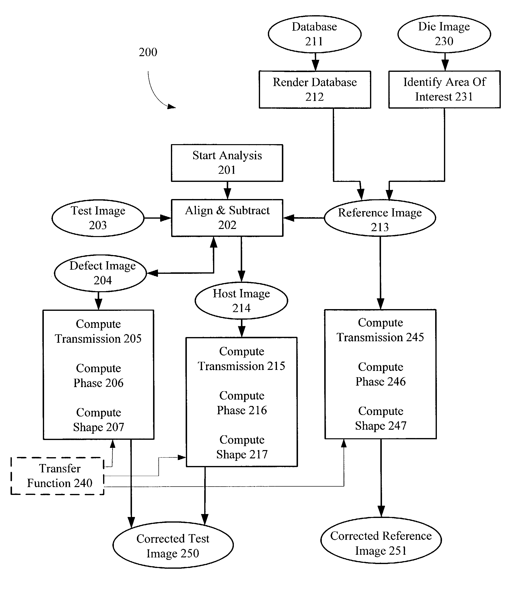
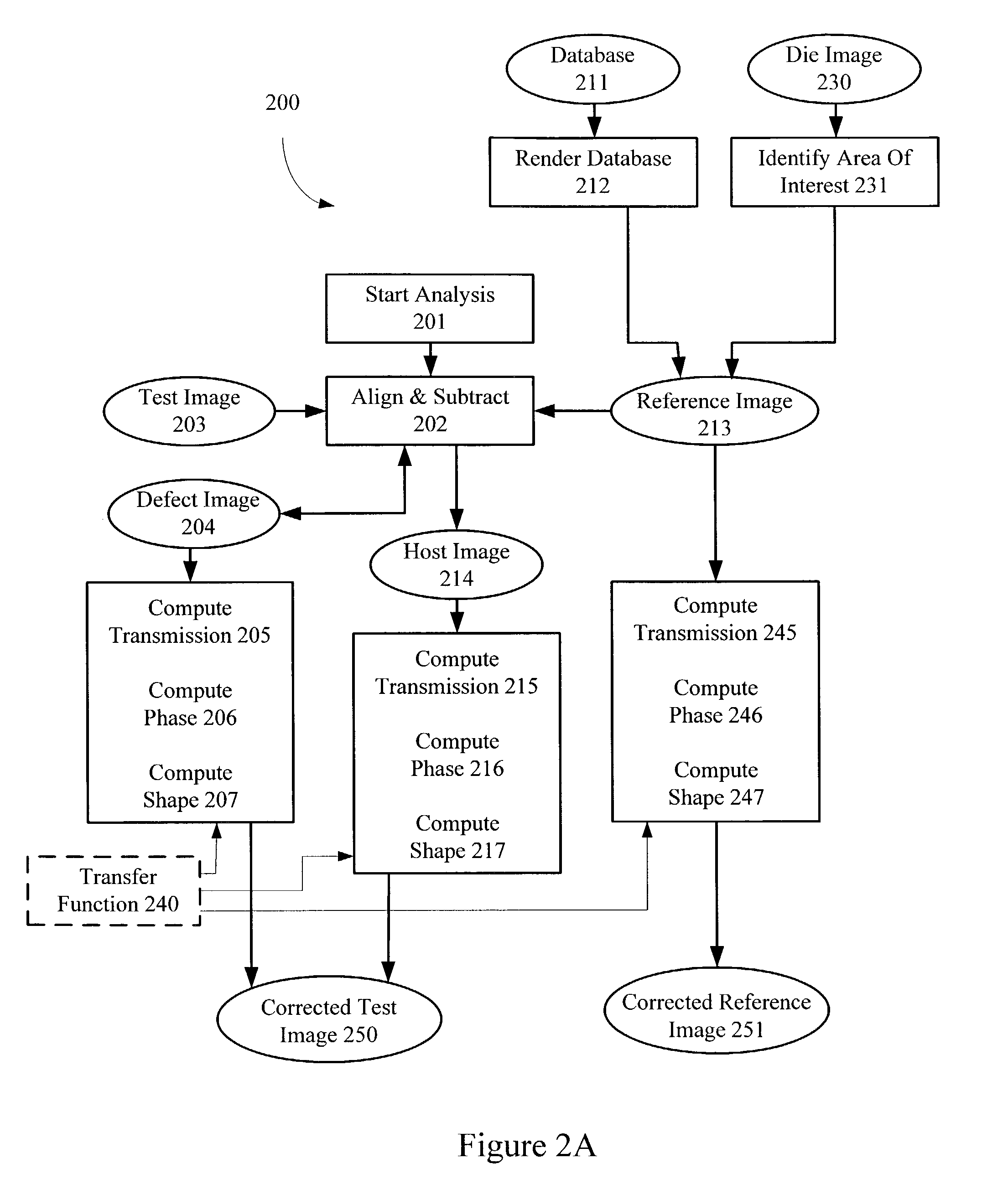
[0069]Although illustrative embodiments of the invention have been described in detail herein with reference to the accompanying figures, it is to be understood that the invention is not limited to those precise embodiments. They are not intended to be exhaustive or to limit the invention to the precise forms disclosed. As such, many modifications and variations will be apparent.

[0070]For example, if neither database nor gray scale information is available, then certain arbitrary phase assignments to the shifters can be made in the host image. Specifically, assuming that no phase conflicts exist in the host image, a first shifter can be assigned one phase (e.g. 0 degrees). At this point, using the assigned phase from the first shifter, a second shifter proximate to the first shifter can be assigned the opposite phase (e.g. 180 degrees). Note that proximate shifters typically define sub-wavelength features (e.g. a transistor gate) and therefore have opposite phases. In other words, t...


PUM

PropertyMeasurementUnit
defectaaaaaaaaaa
defect imageaaaaaaaaaa
transmissionaaaaaaaaaa

Abstract

Masks that include optical proximity correction or phase shifting regions are increasingly being used in the manufacturing process. These masks, either initially or after repair, can have “soft” defects, e.g. phase and/or transmission defects. In accordance with one feature of the invention, soft defect information can be computed from standard test images of a mask. This soft defect information can be used to generate an accurate simulated wafer image, thereby providing valuable defect impact information to a user. Knowing the impact of the soft defect can enable a user to make better decisions regarding the mask. Specifically, a user can now with confidence accept the mask for the desired lithographic process, repair the mask at certain critical locations, or reject the mask, all without exposing a wafer.

Description

BACKGROUND OF THE INVENTION[0001]1. Field of the Invention[0002]This invention relates to the field of integrated circuit manufacturing, and in particular to a method for obtaining soft, e.g. phase or transmission, defect information from masks used in the manufacture of integrated circuits. This information can be used to determine the impact of such soft defects on wafer printability.[0003]2. Description of Related Art[0004]In designing an integrated circuit (IC), engineers can use computer simulation tools to help create a circuit design. The circuit design consists of individual devices coupled together to provide certain functions. To fabricate this circuit in a semiconductor substrate on a wafer, the circuit design is translated into a layout. Computer aided design (CAD) tools can assist layout designers in the task of translating the discrete circuit elements (such as gate electrodes, field oxidation regions, diffusion regions, metal interconnections, etc.) into shapes in the...

Claims


Application Information

Patent Timeline
Patent Type & Authority Patents(United States)
IPC IPC(8): G06K9/00G06F17/50G03F1/00G06T7/00
CPCG06T7/0002G06T7/0069G06T7/001G06T2207/30148G06T7/571
Inventor QIAN, QI-DEPANG, LINYONG
Owner SYNOPSYS INC
Why Eureka
Try Eureka