Method for fabricating a semiconductor devices provided with low melting point metal bumps

Inactive Publication Date: 2006-05-16
NIPPON STEEL MATERIALS CO LTD
View PDF18 Cites 9 Cited by
  • Summary
  • Abstract
  • Description
  • Claims
  • Application Information

AI Technical Summary

Benefits of technology

[0008]An object of the present invention is to provide a semiconductor device provided with low melting point metal bump

Problems solved by technology

The technologies are, therefore, not suited to high density mounting of the semiconductor devices.
However, such bump formation methods must all repeat complicated treatments steps using a mask.
Moreover, in the method of forming the bumps by vapor deposition, a bump material is deposited on portions where the bumps are not to be formed, and the deposition amount thereon is very large.
Moreover, wet plating such as electroplating or electroless plating fouls wafers and cau

Method used


Image

  • Method for fabricating a semiconductor devices provided with low melting point metal bumps
  • Method for fabricating a semiconductor devices provided with low melting point metal bumps
  • Method for fabricating a semiconductor devices provided with low melting point metal bumps

Examples


Embodiment Construction

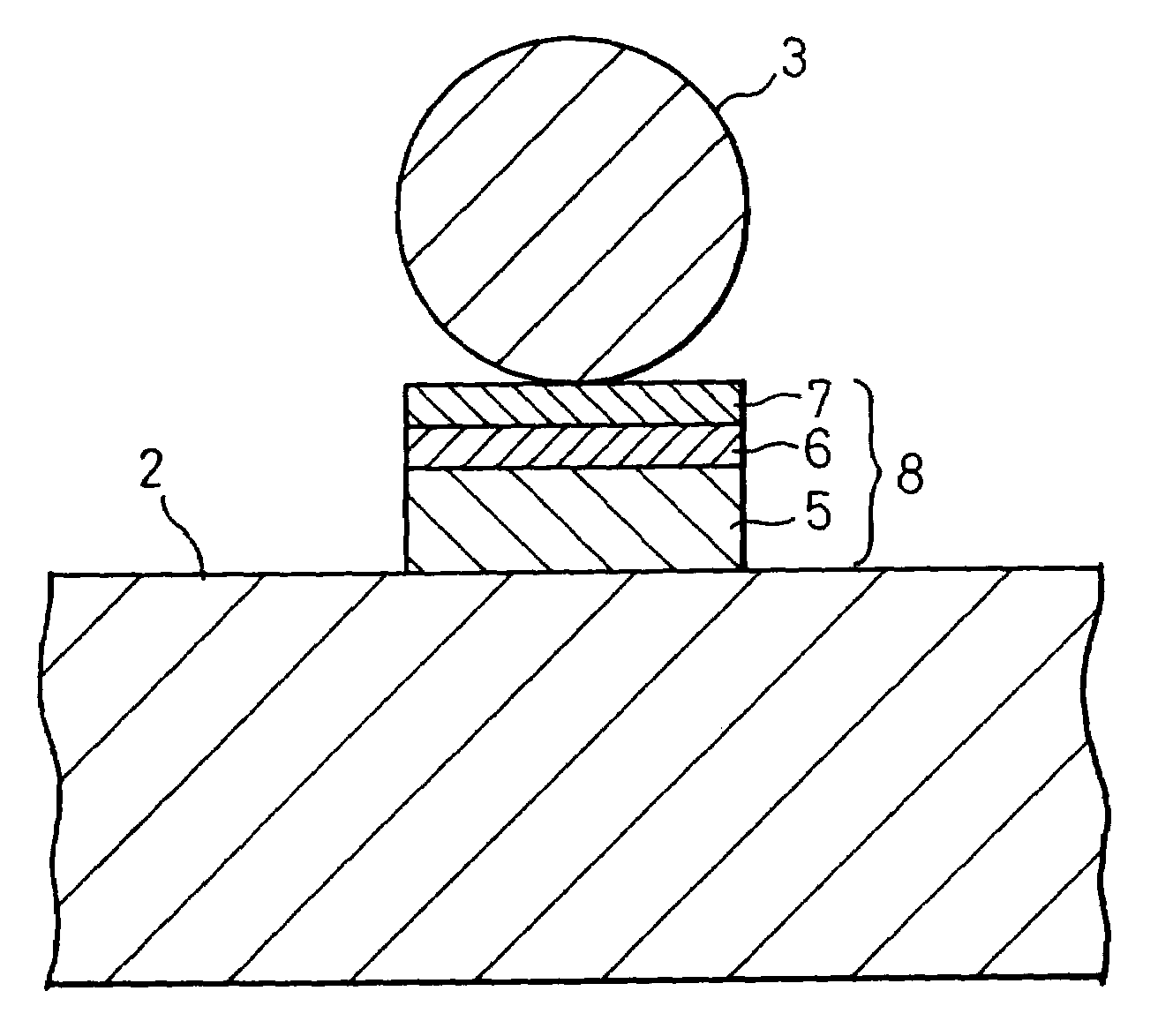
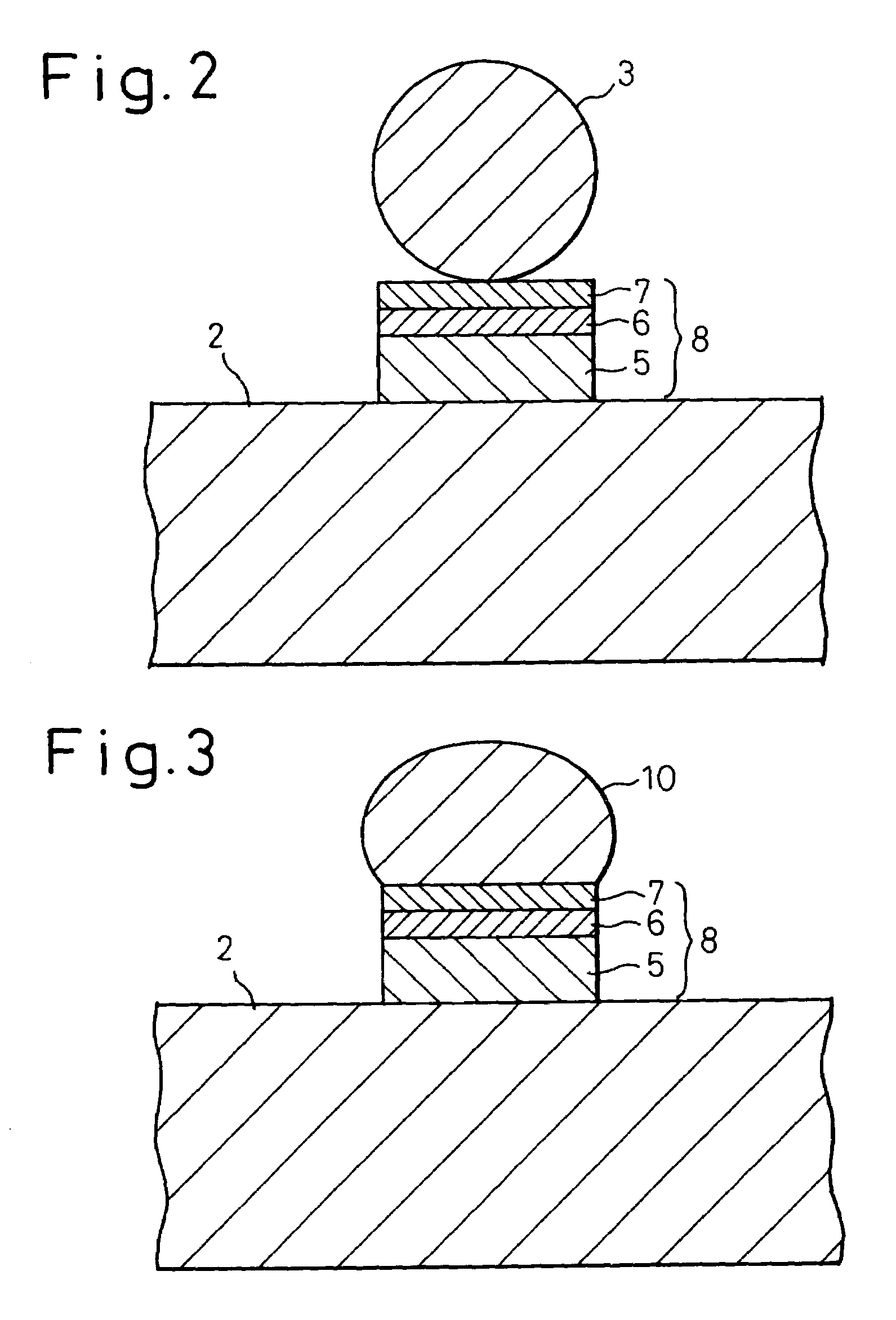
[0028]FIG. 1 shows a semiconductor device 1 of the present invention. The semiconductor device 1 is provided with low melting point metal ball bumps 3 adhesive bonded onto the electrodes (not shown) formed on a surface of a semiconductor chip 2.

[0029]The low melting metal balls 3 can be formed from one of the various solders used for mounting a semiconductor device on a substrate. Examples of the solders include solders of Sn alloys such as a Sn—Pb alloy and a Sn—Ag alloy and solders of Pb alloys such as a Pb—In alloy.

[0030]The electrodes to which the bumps 3 of low melting point metal balls are adhesive bonded can be formed from an electrode material of Cu or a Cu alloy, Al or an Al alloy, or Au or a Au alloy. In the semiconductor device of the present invention, an electrode having a surface area of 900 to 22,500 μm2 is preferably used. That is, when a square electrode is used, one of the sides of the electrode has a dimension of 30 to 150 μm.

[0031]When the electrode material is A...


PUM

PropertyMeasurementUnit
Lengthaaaaaaaaaa
Sizeaaaaaaaaaa
Melting pointaaaaaaaaaa

Abstract

A semiconductor device (1) comprising electrodes formed on a semiconductor chip (2) and bumps (3) which consist of a low melting point metal ball spherically formed and having a given size and which are adhesive bonded to the electrodes (5). The electrodes (5) are formed from an electrode material of Cu or a Cu alloy, Al or an Al alloy, or Au or a Au alloy. When the electrode material is composed of Al or an Al alloy, the electrodes contain, on the electrode material layer of Al or an Al alloy, at least one layer (6) composed of a metal or metal alloy (preferably a metal selected form Ti, W, Ni, Cr, Au, Pd, Cu, Pt, Ag, Sn or Pb, or an alloy of these metals) having a melting point higher than the electrode material. The low melting point metal balls (3) are adhesive bonded to the electrodes (5) preferably with a flux. The low melting point metal balls (3) adhesive bonded to the respective electrodes (3) may also be reflowed to form semispherical bumps (10) before use.

Description

[0001]This application is a divisional application under 37 C.F.R. §1.53(b) of prior application Ser. No. 09 / 254,119 filed Apr. 16, 1999 which is a 35 U.S.C. 371 of PCT / JP97 / 02987 filed Aug. 27, 1997. The disclosures of the specification, claims, drawings and abstract of application Ser. No. 09 / 254,119 and PCT / JP97 / 02987 are incorporated herein by reference.TECHNICAL FIELD[0002]The present invention relates to a semiconductor device provided with low melting point metal bumps and a process for producing the same.BACKGROUND ART[0003]Semiconductor devices have currently been used widely in various fields. The semiconductor devices are usually used by mounting them on substrates. The mounting methods include bonding methods such as tape automated bonding (TAB), wire bonding and flip chip bonding.[0004]The TAB and wire bonding are technologies by which a semiconductor device is mounted on a substrate through leads. The leads are arranged in one row per peripheral side of the semiconduct...

Claims


Application Information

Patent Timeline
IPC IPC(8): H01L21/48B23K31/00H01L23/48H01R43/00H01L21/60H01L23/485H05K3/34
CPCH01L24/03H01L24/11H01L24/05H01L24/13Y10T29/49222H01L2224/0401H01L2224/1148H01L2224/1308H01L2224/13083H01L2224/13111H01L2224/13116H01L2224/13144H01L2224/13147H01L2224/13155H01L2924/01004H01L2924/01005H01L2924/01006H01L2924/01013H01L2924/01014H01L2924/01029H01L2924/01033H01L2924/01046H01L2924/01047H01L2924/0105H01L2924/01061H01L2924/01074H01L2924/01075H01L2924/01078H01L2924/01079H01L2924/01082H01L2924/014H01L2224/0554H01L2224/05001H01L2924/01024H01L2924/01019H01L2924/00013H01L2224/742H01L2224/11334H01L2224/11003H01L2924/00014H01L2924/01049H01L2224/13099H01L24/14H01L24/16H01L24/742H01L24/81H01L24/94H01L2224/0345H01L2224/03828H01L2224/05023H01L2224/05026H01L2224/05027H01L2224/05073H01L2224/05082H01L2224/05083H01L2224/05084H01L2224/05111H01L2224/05116H01L2224/05124H01L2224/05139H01L2224/05144H01L2224/05147H01L2224/05155H01L2224/05164H01L2224/05166H01L2224/05169H01L2224/05171H01L2224/05184H01L2224/05554H01L2224/05555H01L2224/05568H01L2224/05624H01L2224/05644H01L2224/05647H01L2224/11849H01L2224/13013H01L2224/13014H01L2224/14131H01L2224/16227H01L2224/81815H01L2224/94H01L2224/05655H01L2224/05664H01L2224/05611H01L2224/05669H01L2224/11H01L2924/00012
Inventor TATSUMI, KOHEISHIMOKAWA, KENJIHASHINO, EIJI
Owner NIPPON STEEL MATERIALS CO LTD
Why Eureka
Try Eureka