Method for forming a single-crystal silicon layer on a transparent substrate

a technology of transparent substrate and single crystal silicon, which is applied in the direction of layered products, basic electric elements, chemistry apparatus and processes, etc., can solve the problems of poor panel performance, poor suited plastic substrate to the manufacturing process, and high cost, and achieves high thermal expansion coefficient, static and large thermal expansion coefficient, and severe stress

Inactive Publication Date: 2006-05-16
IND TECH RES INST
View PDF10 Cites 57 Cited by
  • Summary
  • Abstract
  • Description
  • Claims
  • Application Information

AI Technical Summary

Problems solved by technology

However, many problems, such as low Tg, arise when using plastic substrates, which hinder the required high temperature process, resulting in poor panel performance.
Moreover, plastic substrates are poorly suited to the manufacturing process, which induces severe stress, static and large thermal expansion coefficient.
However, these flexible metal substrates cannot be incorporated into the current process and equipment.
Glass must be used as a carrier, which is problematic as it requires temporary lamination of metal with glass, which must be separated in a subsequent step.
Current methods for temporary lamination mostly use a high molecular gel, which due to its poor resistance to high temperature, is not suitable for laminating metal and glass.
Coating silver gel, however, is difficult and is not cost effective.
As a result, silver gel is not a satisfactory laminating material.
In addition, current methods cannot directly form a single-crystal silicon layer on a transparent substrate (such as glass), as glass is amorphous and exhibit a melting point of 600° C. If molecular beam epitaxy (MBE) is utilized to directly grow a single-crystal silicon layer, temperature must be between 700 and 800° C., or even higher.

Method used


Image

  • Method for forming a single-crystal silicon layer on a transparent substrate
  • Method for forming a single-crystal silicon layer on a transparent substrate

Examples


example

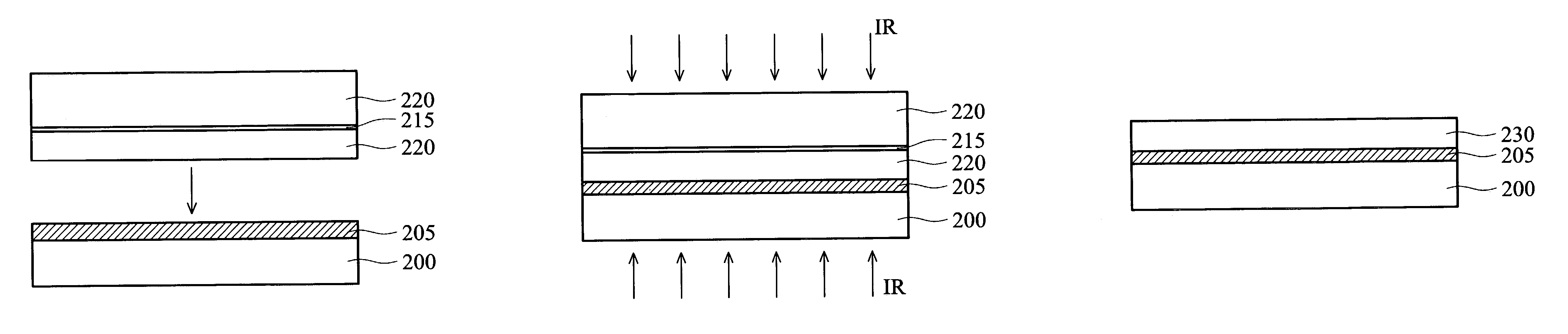
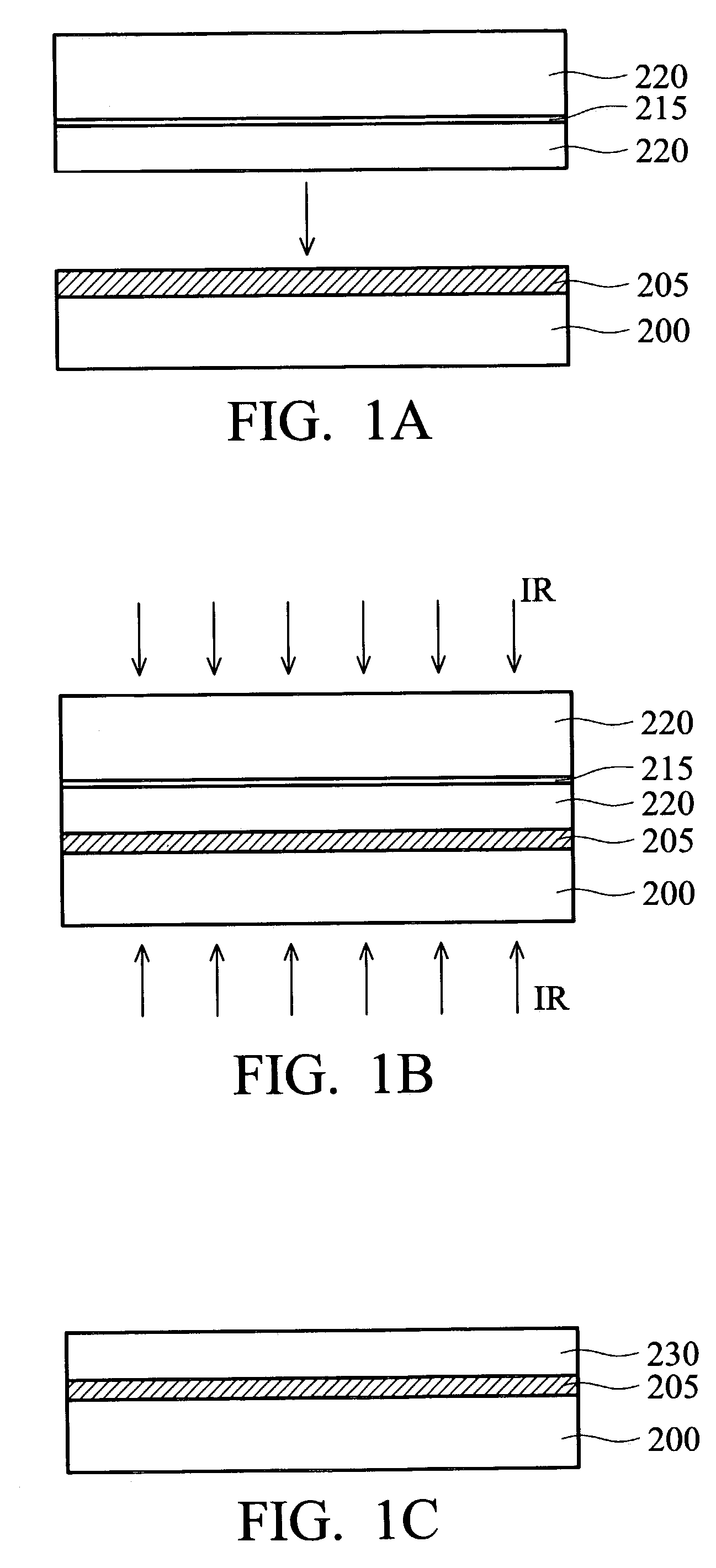
[0015]FIGS. 1A˜1C illustrate cross sections of the embodiment of the invention.

[0016]In FIG. 1A, a transparent substrate 200 having an amorphous silicon layer 205 formed thereon and a silicon wafer 220 with a hydrogen ion layer 215 are provided. In this embodiment, glass is used as the transparent substrate 200. The hydrogen ion layer is formed by doping under the following conditions: dosage 1×10¹⁶˜5×1017 cm−2; energy 10˜1000 keV and doping depth of 0.1˜15 μm.

[0017]Next, as shown in FIG. 1B, the silicon wafer 220 is inverted and laminated onto the amorphous silicon layer 205, followed by exposure to infrared (IR). At this stage, part of the silicon wafer is between the hydrogen ion layer 215 and the amorphous silicon layer 205. IR then passes through the non-infrared absorbent glass substrate 200 and the amorphous silicon layer 205 to cause chemical bonding of the infrared-absorbing single-crystal silicon and the amorphous silicon layer 205. When heating to a certain high temperatu...


PUM

PropertyMeasurementUnit
energyaaaaaaaaaa
depthaaaaaaaaaa
temperatureaaaaaaaaaa

Abstract

A method for forming a, single-crystal silicon layer on a transparent substrate. A transparent substrate having an amorphous silicon layer formed thereon and a silicon wafer having a hydrogen ion layer formed therein are provided. The silicon wafer is then reversed and laminated onto the amorphous silicon layer so that a layer of single-crystal silicon is between the hydrogen ion layer and the amorphous silicon layer. The laminated silicon wafer and the amorphous silicon layer are then subjected to laser or infrared light to cause chemical bonding of the single crystal silicon layer and the amorphous silicon layer and inducing a hydro-cracking reaction thereby separating the silicon wafer is and the transparent substrate at the hydrogen ion layer, and leaving the single-crystal silicon layer on the transparent substrate.

Description

BACKGROUND OF THE INVENTION[0001]1. Field of the Invention[0002]The present invention relates to a lamination method for a transparent substrate, and in particular to a method for forming a single-crystal silicon layer on a transparent substrate.[0003]2. Description of the Related Art[0004]In addition to developing flat panel displays with greater display areas, the lighter, thinner, and more flexible characteristics of flat panel displays have also become desirable. One current trend is to substitute glass substrates with plastic substrates. However, many problems, such as low Tg, arise when using plastic substrates, which hinder the required high temperature process, resulting in poor panel performance. Moreover, plastic substrates are poorly suited to the manufacturing process, which induces severe stress, static and large thermal expansion coefficient. Other alternative substrate materials include metal, or metal alloy, such as aluminum, titanium or similar. Use of these substra...

Claims


Application Information

Patent Timeline
Patent Type & Authority Patents(United States)
IPC IPC(8): H01L21/762H01L23/15C03C27/04
CPCB32B37/00C03C27/046B32B2310/0825Y10S438/977B32B2315/08B32B2311/02H01L2224/83192
Inventor CHANG, CHICH SHANGLEE, CHI-SHENHUANG, SHUN-FACHANG, JUNG FANGHU, WEN-CHIHWANG, LIANG-TANGSHEU, CHAI-YUAN
Owner IND TECH RES INST
Why Eureka
Try Eureka