Charged particle beam apparatus and method for operating the same

a particle beam and apparatus technology, applied in the field of electron microscopes, can solve the problems of slow raster scanning a surface with scanning electron microscopy, inability to establish electrical connection, and failure of whole chip,

Active Publication Date: 2006-05-16
ICT INTEGRATED CIRCUIT TESTING GESELLSCHAFT FUER HALBLEITERPRUEFTECHNIK GMBH
View PDF9 Cites 227 Cited by
  • Summary
  • Abstract
  • Description
  • Claims
  • Application Information

AI Technical Summary

Benefits of technology

[0027]This charged particle beam apparatus is capable of two different modes of operation: a first mode (SEM mode) in which the sample is scanned by a highly focused primary beam, and a second mode (SEEM mode) in which the sample is illuminated by a relatively wide primary beam for parallel, multi-pixel imaging. Thus, the apparatus provides the functions of both, a SEM and a SEEM, but within a single device. Accordingly, an apparatus according to the present embodiment requires much less space and only a single vacuum pump means, compared to two single-functional prior art apparatus which are only capable of either SEM or SEEM. Further to this, the cost of purchase of an apparatus according to the present embodiment is much lower compared to the combined costs of a conventional SEM and SEEM. Therefore, the apparatus according to the present embodiment of the invention is good value for users which need the functions of a SEM as well as of a SEEM but not at the same time.
[0030]This charged particle beam apparatus is also capable of two different modes of operation: a first mode (SEM mode) in which the sample is scanned by a highly focused primary beam, and a second mode (SEEM mode) in which the sample is illuminated by a relatively wide primary beam for parallel, multi-pixel imaging. Accordingly, the apparatus according to the present embodiment provides similar advantages as the apparatus to the embodiment described above. Especially, homogeneous illumination and high current density are specific advantages of this embodiment. The apparatus of the present embodiment utilizes an adapted objective lens to switch between SEM and SEEM mode wherein switching is accomplished by altering the image plane of the objective lens. In SEM mode the objective lens forms an image of the particle source or an intermediate image of the particle source in the focal) plane, thus generating a beam having a very small width in the focal plane. In SEEM mode the objective lens forms an image of the aperture in the focal plane. If the aperture is fully illuminated by the primary beam, a beam having a large width in the focal plane of the objective lens is generated by this mode of operation. However, this is also dependent on the selected magnification which is adjusted by the objective lens.
[0032]The provision of a light source allows additionally for Photo-Electron Emission Microscopy (PEEM) to be accomplished in the present embodiment of the invention. As has been already mentioned above, PEEM may lead to positive charge build-up on insulating surfaces. However, SEEM may lead to negative charge build-up for the aforementioned reasons. Therefore, the apparatus according to the present embodiment may be operated in a combined SEEM / PEEM mode when inspecting insulating surfaces. In this combined SEEM / PEEM mode, the primary beam and the light beam may be adjusted such that the effects of negative / positive charge build-up on insulating surfaces cancel each other and leave the surface in a stable, substantially uncharged state. Thus, also very sensitive structures may be inspected with a largely reduced possibility of damaging them. Moreover, for other materials the incident light beam induces pair production of electrons and holes, thereby generating enhanced surface conductance. The excess charge built up by SEEM inspection could thus be transported away from the illuminated area on the sample surface.
[0035]The above method allows to tap the full potential of the present invention in that a user may select different operation modes and apply them to the same sample without the need of transferring the sample to a different device for each respective mode of operation. Thus, a considerable amount of time and money can be saved since, e.g., the whole device has to be evacuated just once.

Problems solved by technology

If one of these holes or vias becomes clogged, it will be impossible to establish this electrical connection and the whole chip may fail.
However, raster scanning a surface with scanning electron microscopy is slow because each pixel on the surface is collected sequentially.
Moreover, a complex and expensive electron beam steering system is needed to control the beam pattern.
This charge build-up problem may limit the utility of PEEM for imaging insulators.
However, LEEM suffers from a similar charge build-up problem since electrons are directed at the sample surface, but not all of the electrons are energetic enough to leave the surface.
In LEEM, negatively-charged electrons accumulate on the surface, which repels further electrons from striking the sample, resulting in distortions and shadowing of the surface.
In LEEM, it may pose a problem that the surface charges negatively due to the low electron energies.
In Scanning Electron Microscopy (SEM), raster scanning imaging must be utilized which leads to a relatively low throughput because the electron beam is focused to a narrow spot size.
PEEM may suffer from the problem of positive charge build-up on insulating sample target materials because secondary electrons are being knocked off the sample surface by the photons, but no negatively charged particles replace these secondary electrons.
Also, the low energy implies a negative charge build-up because some of the electrons may be energetic enough to enter the sample but are not sufficiently energetic to escape the sample surface.

Method used


Image

  • Charged particle beam apparatus and method for operating the same
  • Charged particle beam apparatus and method for operating the same
  • Charged particle beam apparatus and method for operating the same

Examples


Embodiment Construction

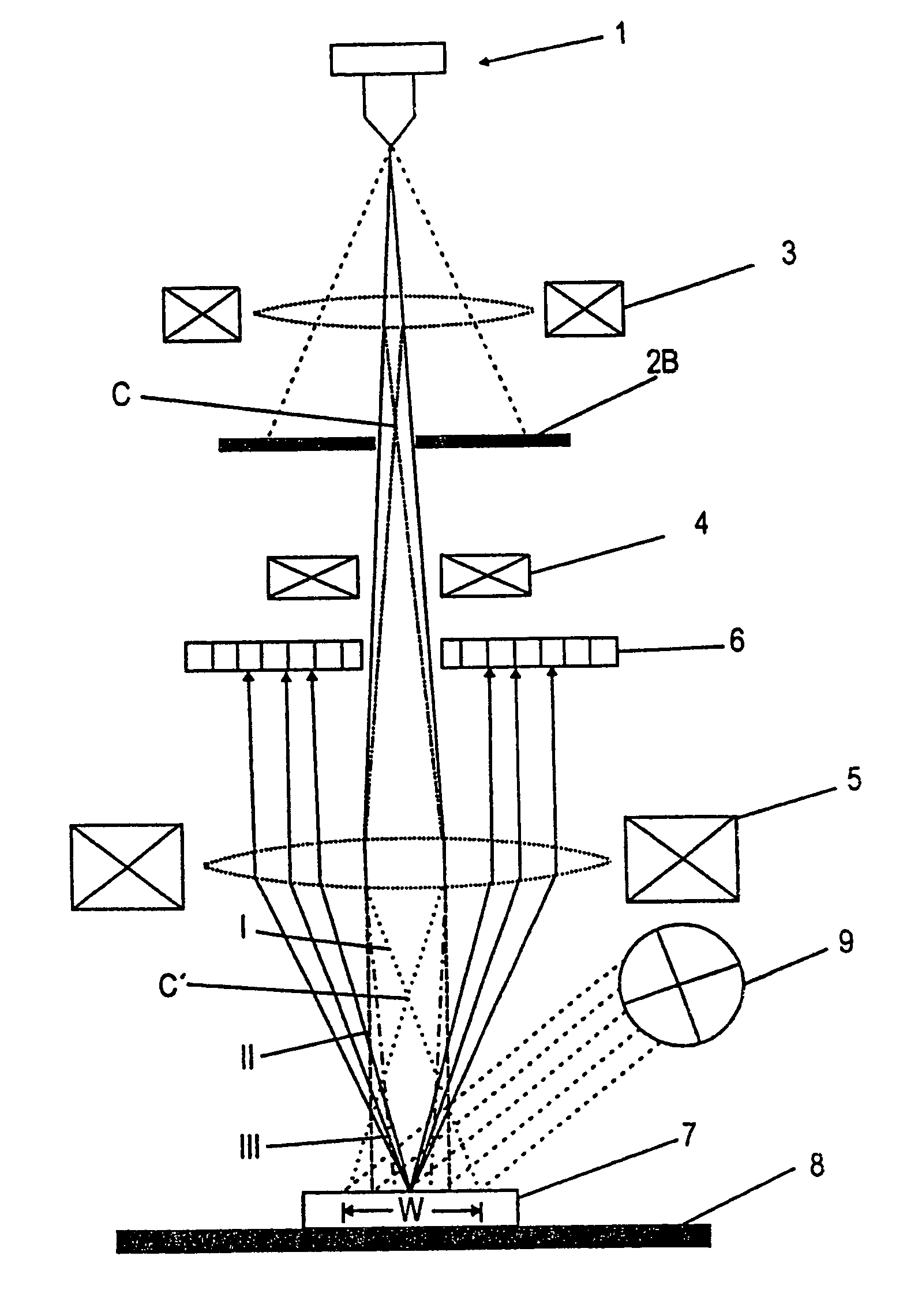
[0046]It is to be understood within the context of the embodiments of the present invention that a charged particle beam is preferably an electron beam. However, this should not be understood as limiting the scope of the present invention since also other charged particles like, e.g. protons or ions, can be used in an apparatus or method according to the present invention.

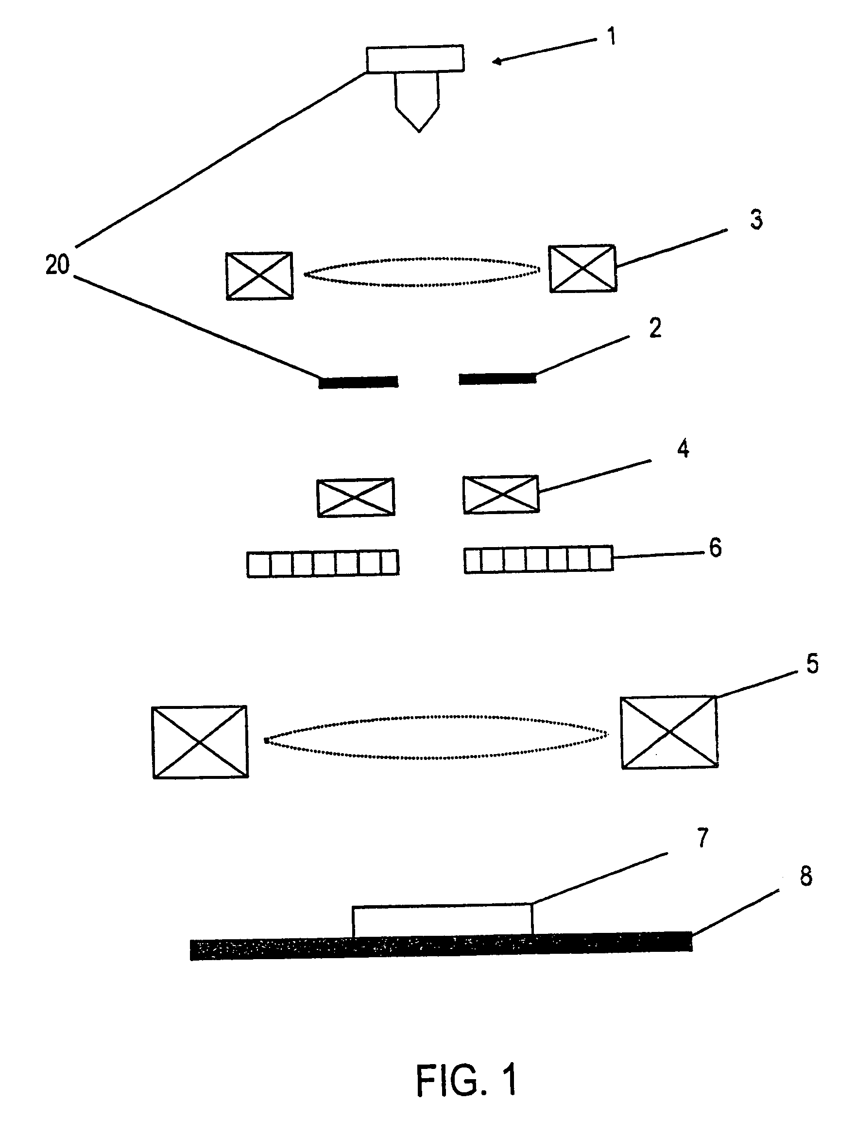
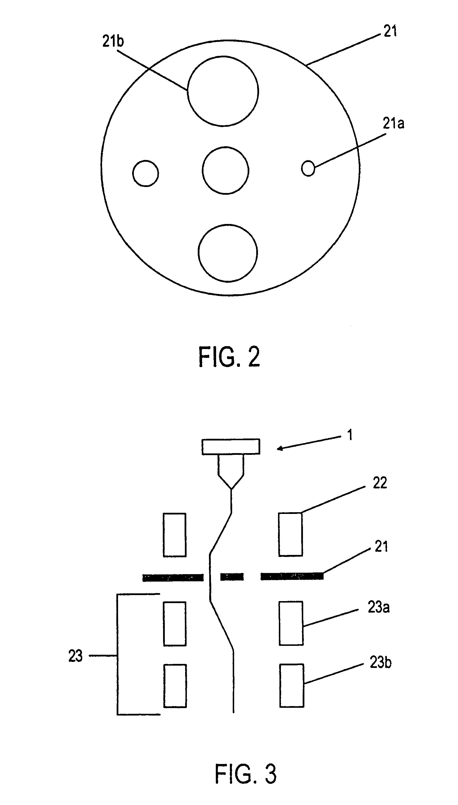
[0047]FIG. 1 shows an electron beam apparatus according to a first embodiment of the present invention. This apparatus comprises a electron source 1, which produces a primary beam of electrons during operation. Typical electron sources are filaments, e.g. made of tungsten, but can also be formed by micro emitter tips or arrays of those.

[0048]In some embodiments according to the present invention, an aperture means 2 is provided which is adapted to switch between two different modes of collimation, a serial imaging mode (SEM mode) and a parallel imaging mode (SEEM mode). In the specific embodiment shown in FIG. 1, t...


PUM


Abstract

A charged particle beam apparatus is provided which comprises a charged particle source for producing a primary beam of charged particles, aperture means for collimating said primary beam of charged particles, wherein said aperture means is adapted to switch between a collimation of said primary beam to a width appropriate for serial imaging of a sample as well as a collimation of said primary beam to a width appropriate for parallel imaging of said sample, a condenser lens for condensing said primary beam of charged particles, scanning means for deflecting said primary beam of charged particles, an objective lens for focusing said condensed primary beam, a sectorized detector for detecting a secondary charged particles. Also, several different operation modes of the beam apparatus are described allowing for serial imaging as well as parallel imaging.

Description

CROSS-REFERENCE TO RELATED APPLICATIONS[0001]This application claims benefit of European Patent Application No. 03 001 048.2, filed Jan. 17, 2003, which is herein incorporated by reference.BACKGROUND OF THE INVENTION[0002]1. Field of the Invention[0003]The present invention relates to a charged particle beam apparatus and a method for operating the same, especially the present invention relates to an electron microscope which may be operated in different modes of operation allowing to switch from a serial imaging mode to a parallel imaging mode and vice versa.[0004]2. Description of the Related Art[0005]A variety of methods have been used to examine microscopic surface structures of semiconductors. These have important applications in the field of semiconductor chip fabrication, where microscopic defects at a surface layer make the difference between a good or bad chip. Holes or vias in an intermediate insulating layer often provide a physical conduit for an electrical connection be...

Claims


Application Information

Patent Timeline
Patent Type & Authority Patents(United States)
IPC IPC(8): H01J37/28H01J37/26
CPCH01J37/26H01J37/265H01J37/28H01J37/285H01J2237/0435H01J2237/049H01J2237/2855H01J2237/2857
Inventor ADAMEC, PAVELDEGENHARDT, RALFFEUERBAUM, HANS-PETERMUNACK, HARRYWINKLER, DIETER
Owner ICT INTEGRATED CIRCUIT TESTING GESELLSCHAFT FUER HALBLEITERPRUEFTECHNIK GMBH
Why Eureka
Try Eureka