Method of photocarrier radiometry of semiconductors

a technology of semiconductors and radiometry, applied in the field of metalological methodologies and instruments, can solve the problems of inability to accurately predict the frequency of the scan signal, early measurements reported without regard, and the interpretation of the ptr signal and computational difficulties, etc., to achieve the effect of reliable reliability, simplified theoretical fit to frequency-scan signals, and high accuracy

Active Publication Date: 2006-05-16
MANDELIS ANDREAS +1
View PDF4 Cites 11 Cited by
  • Summary
  • Abstract
  • Description
  • Claims
  • Application Information

AI Technical Summary

Problems solved by technology

Even so, the ever-present thermal-wave contributions due to direct lattice absorption, followed by non-radiative energy conversion and black-body (thermal infrared) emissions, have resulted in PTR signal interpretational and computational difficulties due to the large number of variables involved [5].
With our development of the PTR methodology as a quantitative technique for non-destructive semiconductor diagnostics, we found [4,5] that early measurements reported without regard to computational uniqueness [17] using simplified theoretical fits to frequency-scan signals cannot be unique and therefore reliable.
However, the presence of even a diminished TW component in high-frequency PTR has been shown [19] to have significant effects on the measured values of the transport parameters, to compromise sensitivity to the carrier wave and to complicate the task of physical interpretation of the signal, thus raising the question of uniqueness of the measured set of solid-state transport parameters.
On the other hand, very tight focusing of the pump laser beam in PMOR tends to give rise to usually undesirable non-linear thermal and electronic effects [15,20,21], besides being unable to sufficiently eliminate the TW component of the signal [22].

Method used


Image

  • Method of photocarrier radiometry of semiconductors
  • Method of photocarrier radiometry of semiconductors
  • Method of photocarrier radiometry of semiconductors

Examples


Embodiment Construction

A) Apparatus

i) Single-Ended Photocarrier Radiometric Instrument

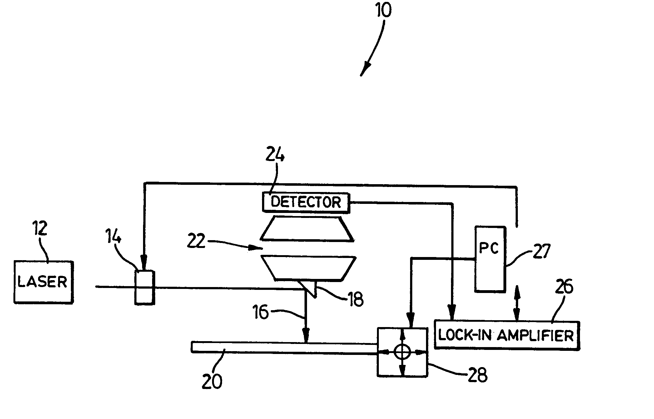
[0046]A schematic diagram of a first embodiment of a novel single-ended photocarrier radiometric instrument for laser PCR for semiconductor characterization is shown at 10 in FIG. 3. The excitation source is a laser 12 capable of producing photons of energy greater than the bandgap of the sample material (hv>EG). An acousto-optic modulator 14 is used to modulate the laser emissions resulting in a harmonic energy source or beam 16 that is directed using mirrors 18 and focused onto the sample 20. A pair of reflecting objectives or other suitable infrared optics, such as two off-axis paraboloidal mirrors, or one paraboloidal mirror collimator and a focusing lens 22 are aligned with the focal point coincident with that of the laser beam and used to collect emitted IR photons from the sample. The collected IR emissions are focused onto a detector 24 after being passed through a filter with a narrow spectral window that ensure...


PUM

PropertyMeasurementUnit
wavelength bandaaaaaaaaaa
poweraaaaaaaaaa
poweraaaaaaaaaa

Abstract

The present invention relates to metrologic methodologies and instrumentation, in particular laser-frequency domain infrared photocarrier radiometry (PCR), for contamination and defect mapping and measuring electronic properties in industrial Si wafers, devices and other semiconducting materials. In particular the invention relates to the measurement of carrier recombination lifetime, τ, carrier diffusivity, D, surface recombination velocities, S, carrier diffusion lengths, L, and carrier mobility, μ, as well as heavy metal contamination mapping, ion implantation mapping over a wide range of dose and energy, and determination of the concentration of mobile impurities in SiO2 layers on semiconductor substrates. The present invention provides a method and complete photocarrier radiometric apparatus comprising novel signal generation and analysis techniques (carrier-wave interferometry) as well as novel instrumental hardware configurations based on the physical principle of photocarrier radiometry. The method comprises (a) optical excitation of the sample with a modulated optical excitation source and (b) detection of the recombination-induced infrared emission while filtering any Planck-mediated emissions. The present invention provides an instrumental method for detecting weak inhomogeneities among semiconducting materials that are not possible to detect with conventional single-ended photocarrier radiometry. The method comprises (a) irradiating both sides of the sample with modulated optical excitation sources that are 180 degrees out of phase with respect to one another and (b) monitoring the diffusion of the interfering, separately generated carrier waves through the corresponding recombination-induced IR emissions for PCR detection, or the use of an alternative detection scheme that monitors a sample property dependent on the carrier wave transport in the sample.

Description

CROSS REFERENCE TO RELATED U.S APPLICATION[0001]This patent application relates to, and claims the priority benefit from, U.S. Provisional Patent Application Ser. No. 60 / 454,347 filed on Mar. 14, 2003, which is incorporated herein by reference in its entirety.FIELD OF INVENTION[0002]The present invention relates to metrologic methodologies and instrumentation, in particular laser infrared photocarrier radiometry (PCR), for contamination and defect mapping and measuring electronic properties in industrial Si wafers, devices and other semiconducting materials. In particular the invention relates to the measurement of carrier recombination lifetime, τ, carrier diffusivity, D, surface recombination velocities, S, and carrier diffusion lengths, L.BACKGROUND OF INVENTION[0003]In recent years the development of laser-induced infrared photothermal radiometry (PTR) of semiconductors in our laboratory [1–9] and elsewhere [10] as a quantitative methodology for the measurement of transport prop...

Claims


Application Information

Patent Timeline
Patent Type & Authority Patents(United States)
IPC IPC(8): G01J5/02G01N21/17
CPCG01N21/17
Inventor MANDELIS, ANDREASSHAUGHNESSY, DERRICKBATISTA, JERIAS ALVESGARCIA, JOSE A.
Owner MANDELIS ANDREAS
Why Eureka
Try Eureka