Semiconductor integrated circuit device and a method of manufacturing the same

a technology of integrated circuit and semiconductor, applied in the field of semiconductor integrated circuit devices, can solve the problems of reliability of conventional second memory cells, large drawbacks in logic-mixed flash memory modules which need high-speed reading, and small drain current at the time of reading operation in low threshold voltage state, so as to prevent undesired charge leakage, reduce the possibility of undesired charge leakage developed via the second gate electrode, and achieve satisfactory charge pull-out or drawing performance.

Inactive Publication Date: 2006-05-16
RENESAS ELECTRONICS CORP
View PDF25 Cites 62 Cited by
  • Summary
  • Abstract
  • Description
  • Claims
  • Application Information

AI Technical Summary

Benefits of technology

[0019]An object of the present invention is to provide a technology that is capable of reading memory information at high speed from a nonvolatile memory cell transistor formed in a semiconductor integrated circuit device.
[0113]A semiconductor integrated circuit device according to a still further aspect of the present invention has a basic structure similar to ones described up to now, i.e., a memory cell transistor provided on a semiconductor substrate, and an access circuit therefor provided thereon. The memory cell transistor includes a pair of memory electrodes, one of which serves as a source electrode and the other serves as a drain electrode, and a channel region interposed between the pair of memory electrodes, both of which are provided in a first well region of the semiconductor substrate, and includes, on the channel region, a first gate electrode disposed near the corresponding memory electrode with a first gate insulating film interposed between the first gate electrode and the channel region, and a second gate electrode formed on the channel region with a second insulating film and a charge storage region and electrically isolated from the first gate electrode. Further, the first gate electrode is different in conductivity type from the second gate electrode. An initial threshold voltage as viewed from the first gate electrode and an initial threshold voltage as viewed from the second gate electrode are determined so as to be desirable in terms of a read operation. For example, an initial threshold voltage as viewed from the second gate electrode is set low in the case of a read operation, and the voltage to be applied to the second gate electrode is set to a low voltage like a circuit's ground voltage upon reading, thereby making it possible to avoid a reduction in data retention performance due to a so-called word line disturbance.

Problems solved by technology

A first problem resides in the fact that the drain current at the time of a reading operation in a low threshold voltage state is small.
This problem results in a large drawback in a logic-mixed flash memory module which needs high-speed reading at about 100 MHz, for example.
A second problem relates to the reliability of the conventional second memory cell.
Therefore, a reduction in in-film field intensity was considered to be a cause of this problem.

Method used


Image

  • Semiconductor integrated circuit device and a method of manufacturing the same
  • Semiconductor integrated circuit device and a method of manufacturing the same
  • Semiconductor integrated circuit device and a method of manufacturing the same

Examples


Embodiment Construction

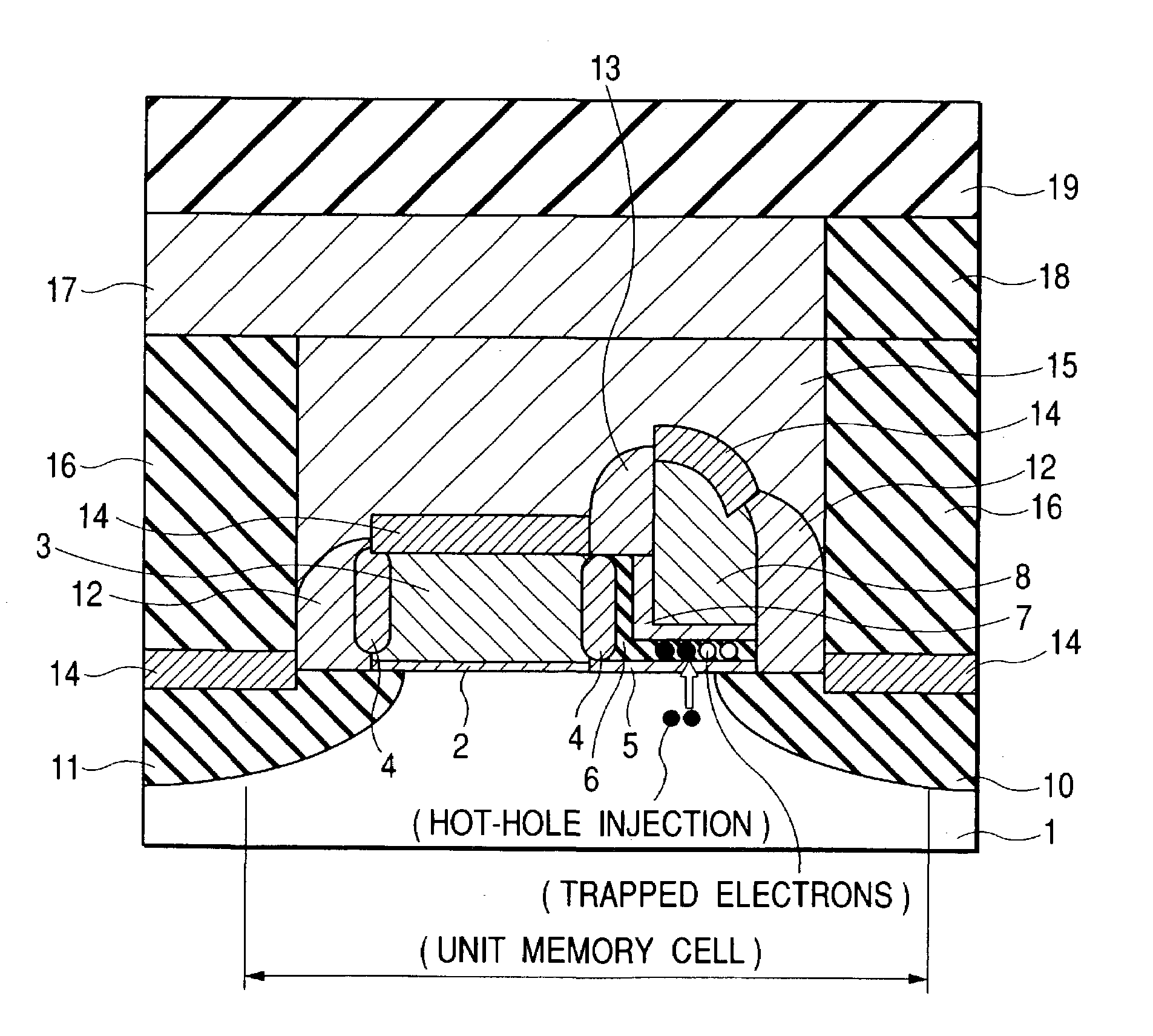
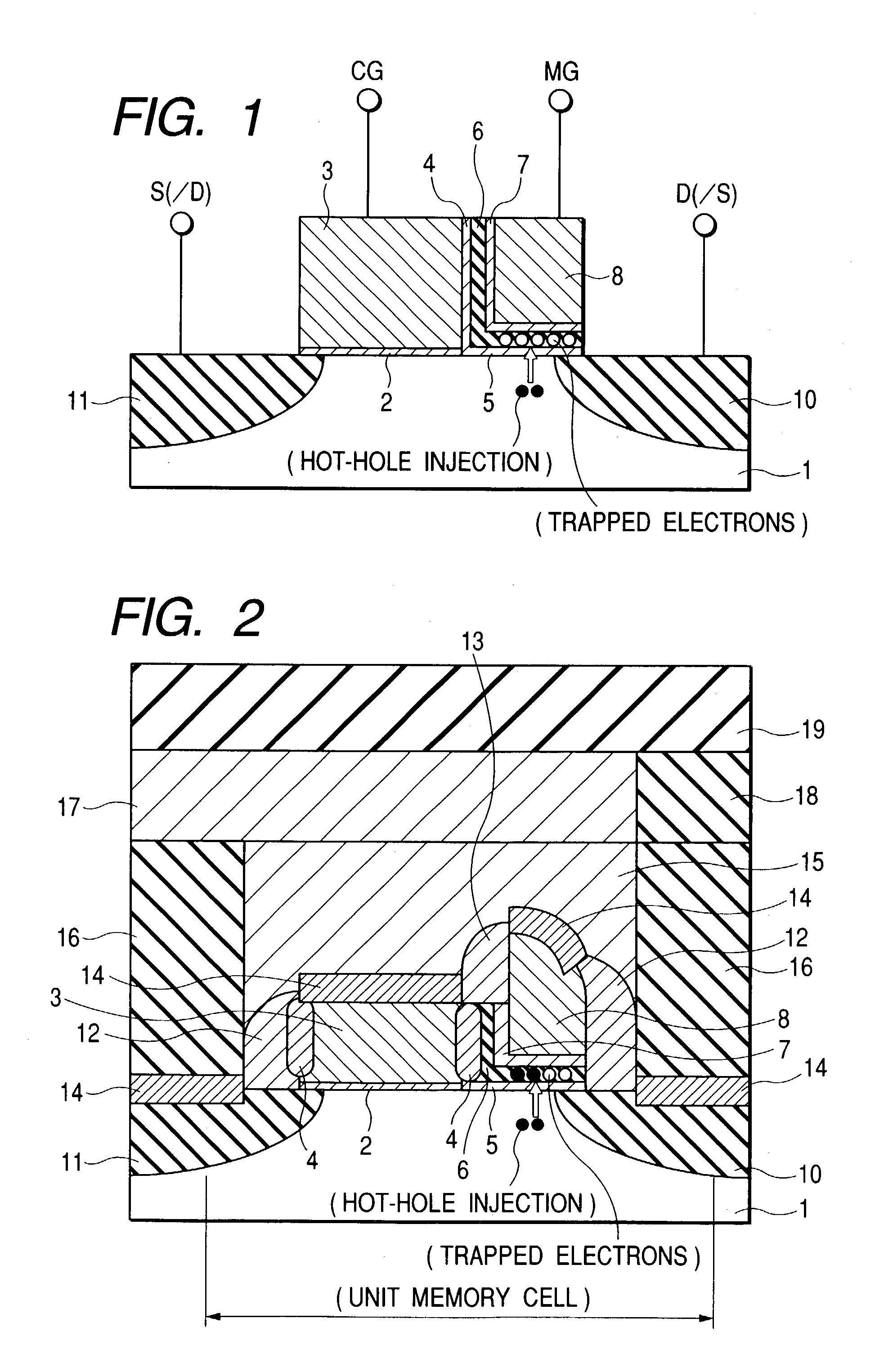
[0180]Preferred embodiments of the present invention will be described in detail with reference to the accompanying drawings. Incidentally, components having the same function in all of the drawings are respectively identified by the same reference numerals, and their repetitive description will be omitted. In the following description, a MOS (Metal Oxide Semiconductor) transistor (also simply described as “MOS”) will be used as one example of MIS transistors (or MISFET), which are generic names for insulated gate field effect transistors.

[0181]>

[0182]A nonvolatile memory cell transistor (also simply called a “memory cell”) applied to a semiconductor integrated circuit device according to the present invention is illustrated in FIG. 1 in the form of a vertical cross-section. A first structural viewpoint related to the memory cell transistor resides in writing and erasure operations based on electron- and hot-hole injection, and a split gate structure. Namely, the memory cell transis...


PUM


Abstract

The memory cell transistor includes, in a first well region, a pair of memory electrodes, one of which serves as source electrode and the other serves as a drain electrode and a channel region interposed between the pair of memory electrodes. There is, on a channel region, a first gate electrode disposed near its corresponding memory electrode with an insulating film interposed therebetween, and a second gate electrode disposed through insulating films and a charge storage region and electrically isolated from the first gate electrode. A first negative voltage is applied to the first well region to form a state of a reverse bias greater than or equal to a junction withstand voltage between the second gate electrode and the memory electrode near the second gate electrode, thereby enabling injection of hot electrons into the charge storage region and injection of electrons from the well region to the charge storage region.

Description

TECHNICAL FIELD[0001]The present invention relates in general to a semiconductor integrated circuit device having a nonvolatile memory cell transistor (nonvolatile memory element), and to a method of manufacture thereof; and, more particularly, the invention relates, for example, to a technology that is effective when applied to a semiconductor integrated circuit device equipped with an on-chip nonvolatile memory, using a nonconductive charge trap film in an information retention region together with a CPU (Central Processing Unit).BACKGROUND OF THE INVENTION[0002]As a memory device for storing data or program-configured data, attention has recently been focused on a flash EEPROM (hereinafter called a “flash memory”), which is defined as a nonvolatile memory device that is capable of electrically erasing data that is stored in predetermined units in batch form and of electrically writing data. In a flash memory, each memory cell is made up of an electrically erasable and programmabl...

Claims


Application Information

Patent Timeline
Patent Type & Authority Patents(United States)
IPC IPC(8): H01L29/76G11C16/04G11C16/10G11C16/14G11C16/26H01L21/8234H01L21/8246H01L21/8247H01L27/088H01L27/10H01L27/105H01L29/788H01L29/792
CPCB82Y10/00H01L29/792H01L21/28282H01L27/0207H01L27/105H01L27/115H01L27/11521H01L27/11526H01L27/11546H01L27/11568H01L27/11573H01L29/42344H01L29/66833G11C16/14G11C16/26G11C16/34H01L21/28273H01L29/66825G11C16/10H01L2924/0002H01L29/40114H01L29/40117H10B69/00H10B41/30H10B41/40H10B41/49H10B43/30H10B43/40H01L2924/00H01L29/42328H01L29/45H10B43/35H01L23/535H01L29/42368G11C16/0466H01L29/4975H01L29/513H01L29/518
Inventor SHUKURI, SHOJI
Owner RENESAS ELECTRONICS CORP
Why Eureka
Try Eureka