
Fault detection system

a fault detection and fault technology, applied in the field of fault detection systems, can solve the problems of increasing the reliability of a semiconductor, destroying a semiconductor module, and preventing the system from working, and achieve the effect of simple structur

Inactive Publication Date: 2006-05-16
HITACHI LTD
View PDF8 Cites 8 Cited by
  • Summary
  • Abstract
  • Description
  • Claims
  • Application Information

AI Technical Summary

Benefits of technology

[0008]It is an object of the present invention to provide a simply structured, low-cost fault detection system capable of directly detecting the deterioration of a semiconductor module without using many detection means.

Problems solved by technology

One of the important problems of an inverter is to increase the reliability of a semiconductor module in the main circuit.
Those problems sometimes result in the sudden destruction of a semiconductor module during system operation and stop the system.
One of main fault modes of a semiconductor module is a semiconductor chip destruction caused by an insufficient radiation.
This is caused by a long-time thermal fatigue that generates cracks in the soldering layer attaching the semiconductor chip onto the radiation fin, and those cracks sometimes result in the semiconductor chip being improperly attached.
Similar problems have arisen in the semiconductor module of an integrated circuit, such as a CPU, where processing power is significantly increased and the heat generation is a problem.
The method described in JP-A-7-14948 requires a plurality of temperature sensors, making the detection means in an inverter, composed of a plurality of semiconductor modules, more costly and complicated.
Although the method described in JP-A-8-126337 shows the history of temperatures that caused cracks in the soldering layer, it does not show the degree of deterioration.
Another problem is that, because the deterioration of semiconductor modules varies widely, a semiconductor module is sometimes destroyed before the thermal stress reaches the upper limit value.
In the latter case, replacing the semiconductor module when the estimated life terminates does not exploit the full capabilities of the semiconductor module.

Method used


Image

  • Fault detection system
  • Fault detection system
  • Fault detection system

Examples


first embodiment

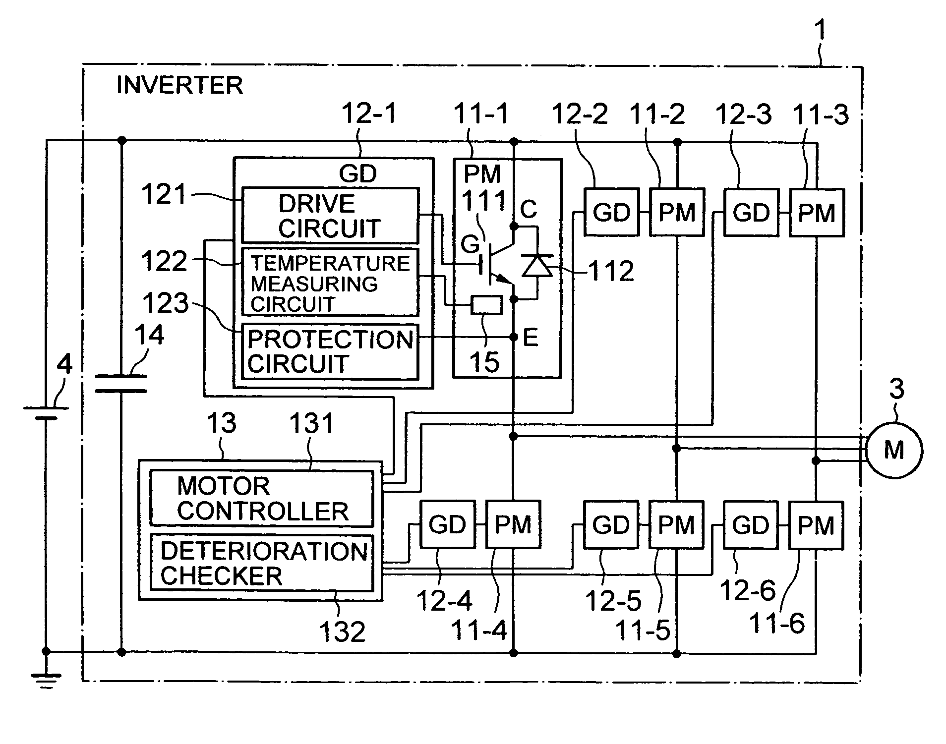
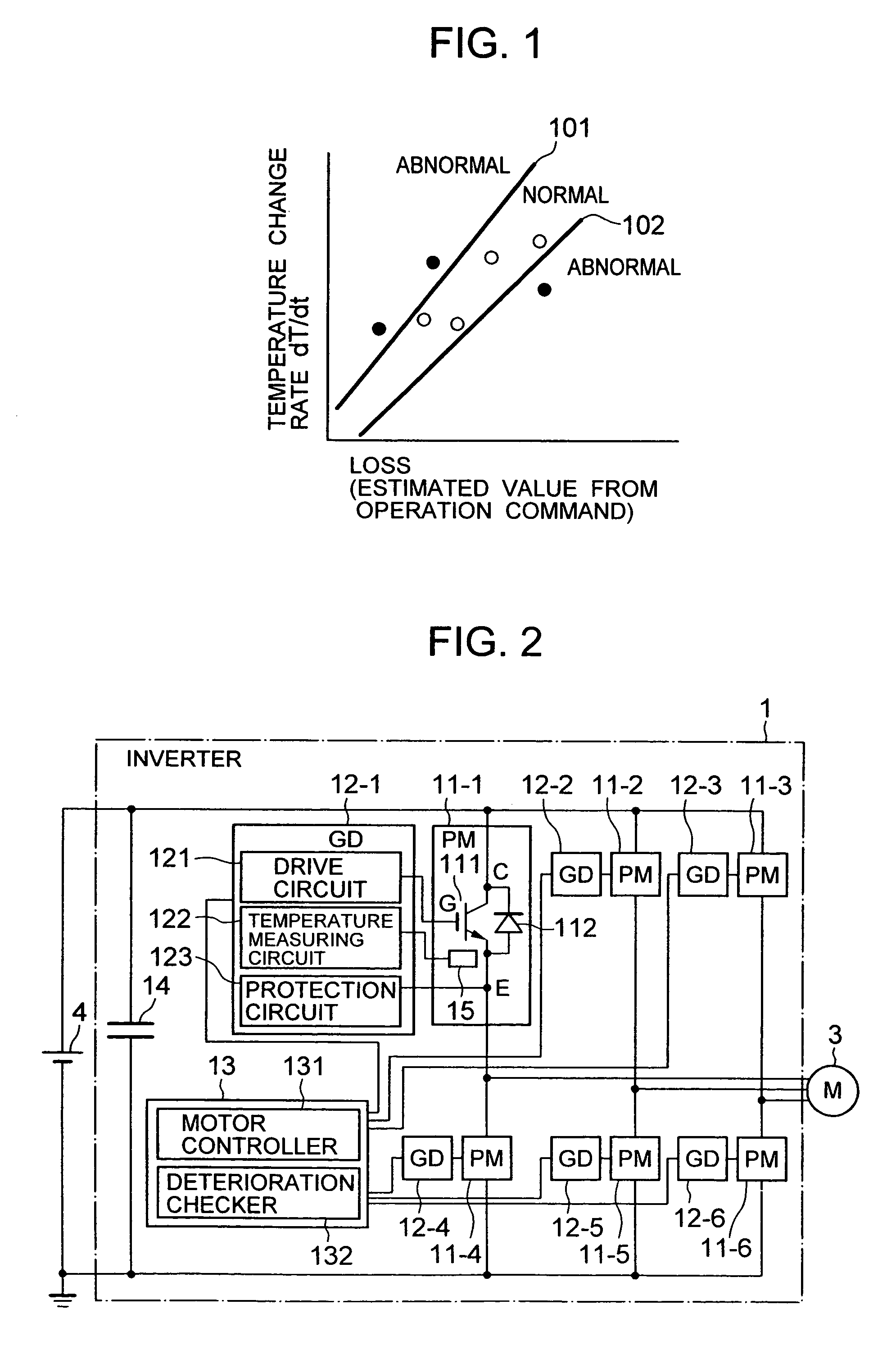
[0043]Referring to FIG. 2, the configuration of a fault detection system of semiconductor modules according to the present invention that is applied to an inverter will be described. An inverter 1 in this embodiment comprises six semiconductor modules 11-1–11-6 each of which is a power module (PM), gate drive circuits (GD) 12-1–12-6, a control circuit 13, and a capacitor 14. This inverter transforms the power of a DC power supply 4 into a three-phase AC power to drive a motor 3.

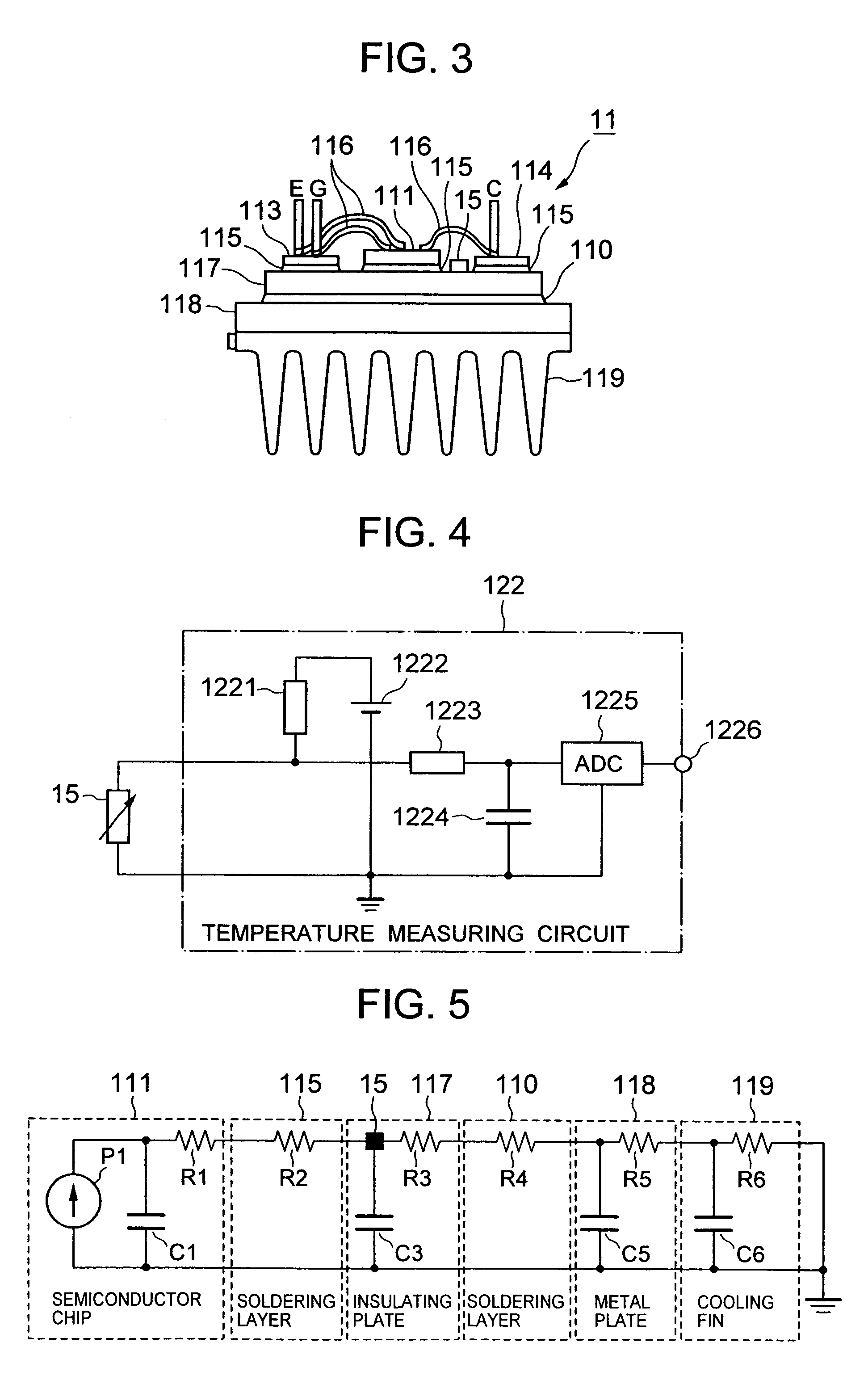
[0044]The semiconductor module 11 comprises an insulated-gate bipolar transistor (IGBT) 111 and a diode 112, where C is the collector terminal, E is the emitter terminal, and G is the gate terminal. A temperature sense device 15 is attached to the semiconductor module 11. Although the detailed configuration of the semiconductor modules 11-2–11-6 is omitted, those modules have the same configuration as that of the semiconductor module 11-1.

[0045]The gate drive circuit (GD) 12 comprises a drive circuit 121 that...

seventh embodiment

[0086]FIG. 22 shows the configuration of an inverter 1 in the present invention. In each of six semiconductor modules 11′-1–11′-6, only an IGBT and a diode are installed but a temperature sense device 15 is not, and those modules are installed on a cooling unit 100 on which the temperature sense device 15 is installed. In addition, a temperature measuring circuit 122 is independent of a gate drive circuit 17′.

[0087]FIG. 23 is an external view of this semiconductor module 11′ and the cooling unit 100. The heat generated by the semiconductor modules 11′ is radiated into air by the cooling unit 100. The cooling unit 100 has the temperature sense device 15 installed. The temperature measuring circuit 122 measures the temperature using the signal sent from the temperature sense device 15. The control circuit 13 checks deterioration based on this temperature information. It is possible to detect deterioration because, in this embodiment, the temperature rise rate changes if any one of six...


PUM


Abstract

A fault detection system detecting malfunctions or deteriorations, which may result in an inverter fault, is provided. The system has a temperature sensor installed on a semiconductor module to monitor a temperature rise rate. It is judged that an abnormal condition has occurred if the thermal resistance is increased by the deterioration of a soldering layer of the semiconductor module or by drive circuit malfunctions and, as a result, the relation between an operation mode and the temperature rise rate falls outside a predetermined range.

Description

[0001]This application is a continuation of application Ser. No. 10 / 098,459 filed Mar. 18, 2002, now U.S. Pat. No. 6,759,964.BACKGROUND OF THE INVENTION[0002]The present invention relates to a fault detection system that detects a fault or deterioration in a semiconductor module, particularly in an inverter, and to the operation method of an inverter system with a plurality of inverters.[0003]An inverter has been used widely, for example, to save energy in, and increase the functionality of, the power system of a train. One of the important problems of an inverter is to increase the reliability of a semiconductor module in the main circuit. A conventional way to ensure reliability is to make a fatigue test to evaluate performance in order to prevent the semiconductor module from being destroyed during system operation. However, the life of a semiconductor module depends largely on the usage condition and varies widely according to the semiconductor modules. Those problems sometimes ...

Claims


Application Information

Patent Timeline
Patent Type & Authority Patents(United States)
IPC IPC(8): G08B17/02G08B17/06H02H3/24H02H5/04H02M1/00H02M7/00H02M7/48
CPCH02M7/00H01L2224/48091H01L2224/48472H01L2224/73265H01L2924/13055H01L2924/1305H01L2924/00014H01L2924/00
Inventor SATO, YUTAKANAGASU, MASAHIROISHIKAWA, KATSUMISAITO, RYUICHIINARIDA, SATORU
Owner HITACHI LTD
Learn More