Reflective semiconductor optical amplifier

a semiconductor optical amplifier and reflector technology, applied in the direction of semiconductor lasers, optical elements, instruments, etc., can solve the problems of large power consumption of semiconductor optical amplifiers, unfavorable high frequency response characteristics, unstable output of mode-locked fabry-perot laser diodes (fp-ld), etc., to achieve high gain and reduce power consumption

Inactive Publication Date: 2006-05-16
SAMSUNG ELECTRONICS CO LTD
View PDF4 Cites 16 Cited by
  • Summary
  • Abstract
  • Description
  • Claims
  • Application Information

AI Technical Summary

Benefits of technology

[0007]The present invention has been made to solve the above-mentioned problems occurring in the prior art and provides additional advantages, by providing a reflective semiconductor optical amplifier, having high gain even under conditions of low operating current and reduced power consumption due to low threshold current, for use as a light source for amplifying, modulating, and transmitting signals in a WDM-PON.
[0008]Another aspect of the present invention is to provide a reflective semiconductor optical amplifier having superior high frequency response characteristic.
[0009]In one embodiment, there is provided a reflective semiconductor optical amplifier that includes a substrate, an optical waveguide with a buried heterostructure formed by sequentially laminating a lower cladding, an active layer, and an upper cladding on the substrate, the heterostructure including a straight line waveguide region, a curved waveguide region, and a tapered waveguide region; a current blocking layer formed around the optical waveguide to prevent electric current from flowing to a region other than the active layer of the optical waveguide. A trench is formed by selectively etching portions of the current blocking layer and the substrate around the optical waveguide in order to reduce parasitic capacitance due to electric current leaked around the active layer. A window region formed on one end of the tapered waveguide region, and an anti-reflection surface formed on one end of the window region. A high-reflection surface formed on one end of the straight line waveguide region to reflect inputted light.

Problems solved by technology

Yet, the output of the mode-locked Fabry-Perot laser diode (FP-LD) may be unstable, because its locking characteristics become deteriorated when temperature or environmental change modifies the wavelength of oscillation mode.
However, since general semiconductor optical amplifiers have driving current and threshold current higher than those of FP-LDs, the semiconductor optical amplifiers consume a large amount of power.
In addition, since the semiconductor optical amplifiers have long length and do not oscillate, they have they exhibit an unfavorable high frequency response characteristic.
Reflective semiconductor optical amplifiers having general structures are therefore unsuitable as light sources by which to amplify, modulate, and transmit signals in the WDM-PONs.

Method used


Image

  • Reflective semiconductor optical amplifier
  • Reflective semiconductor optical amplifier
  • Reflective semiconductor optical amplifier

Examples


Embodiment Construction

[0023]An embodiment according to the present invention is described below with reference to the accompanying drawings, with detailed description of known functions and configurations being omitted for clarity and simplicity of presentation.

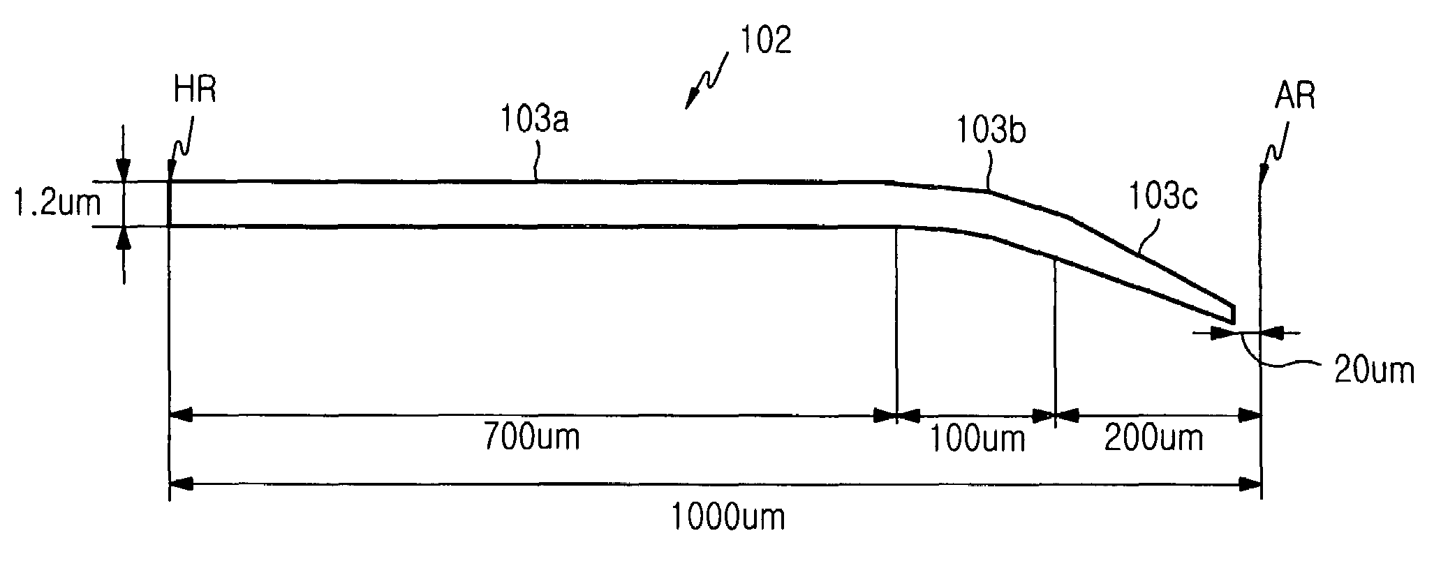
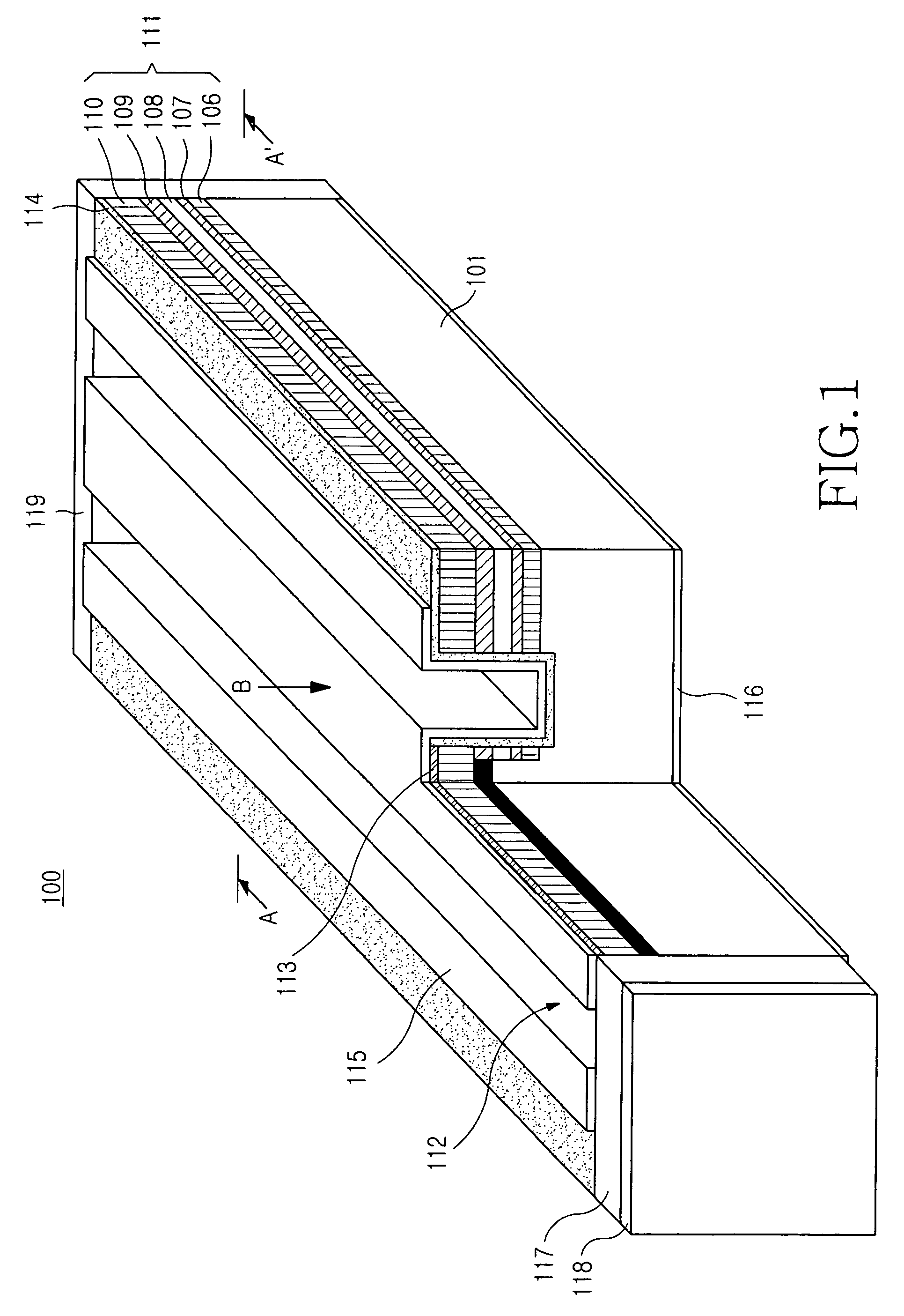
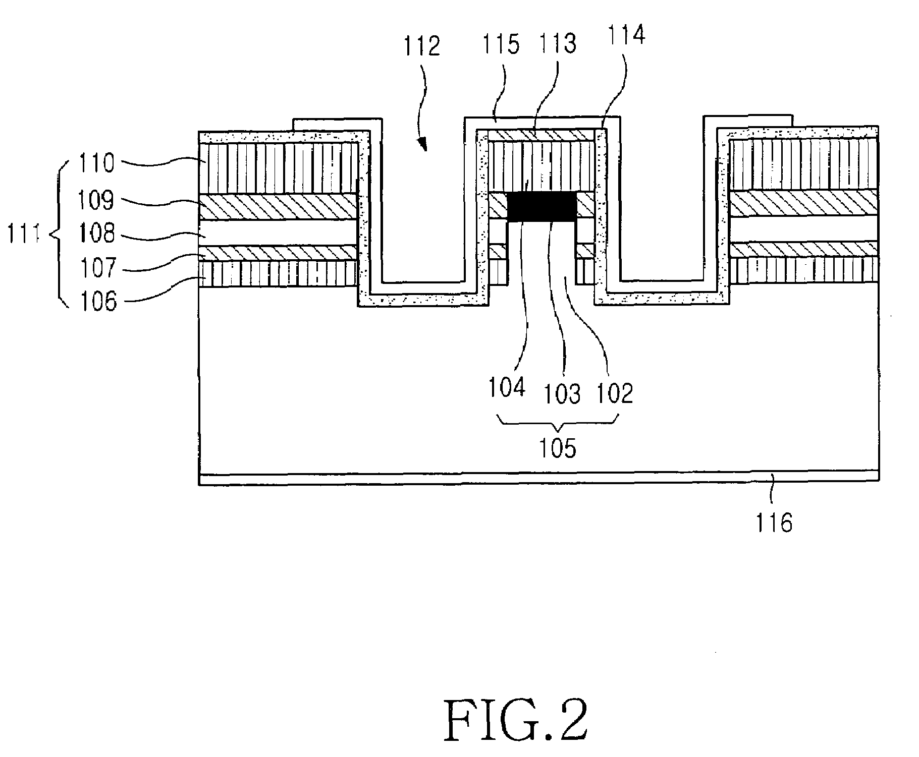
[0024]FIG. 1 is a perspective view showing, by way of illustrative and non-limitative example, a reflective semiconductor optical amplifier according to one embodiment of the present invention, and FIG. 2 is a sectional view taken along line A–A′ in FIG. 1. In FIGS. 1 and 2, thickness, width, and length of composition material layers are inexactly drawn, and do not show actual size or proportional sizes of these material layers.

[0025]Referring to FIGS. 1 and 2, the reflective semiconductor optical amplifier 100 according to the present invention includes a substrate 101, an optical waveguide 105, a current blocking layer 111, a trench 112, an ohmic contact layer 113, a passivation layer 114, an upper electrode 115, a lower electrode 116, a window ...


PUM


Abstract

A reflective semiconductor optical amplifier includes a substrate, a waveguide with a buried heterostructure formed by sequentially laminating a lower cladding, an active layer, and an upper cladding on the substrate, the waveguide including, sequentially, respective straight line, curved and tapered waveguide regions. A current blocking layer surrounds the waveguide to prevent electric current from flowing outside the active layer. Selectively etching portions of the current blocking layer and the substrate around the waveguide forms a trench to reduce parasitic capacitance. Further features include a window region on one end of the tapered waveguide region, an anti-reflection surface on one end of the window region, and a high-reflection surface on one end of the straight line waveguide region.

Description

CLAIM OF PRIORITY[0001]This application claims priority to an application entitled “Reflective Semiconductor Optical Amplifier,” filed in the Korean Intellectual Property Office on Feb. 19, 2004 and assigned Serial No. 2004-11157, the contents of which are hereby incorporated by reference.BACKGROUND OF THE INVENTION[0002]1. Field of the Invention[0003]The present invention relates to a semiconductor optical amplifier, and more particularly to a reflective semiconductor optical amplifier suitable for a wavelength-division-multiplexing passive-optical-network (hereinafter, referred to as a “WDM-PON”). The amplifier has high gain even under conditions of low operating current and low threshold current, thereby affording reduced power consumption.[0004]2. Description of the Related Art[0005]From among the WDM-PON light sources being considered for future ultra high speed optical subscriber networks, mode-locked Fabry-Perot lasers with incoherent lights or wavelength-seeded reflective se...

Claims


Application Information

Patent Timeline
Patent Type & Authority Patents(United States)
IPC IPC(8): H01S3/00G02B6/12H01S5/028H01S5/10H01S5/16H01S5/227H01S5/50
CPCH01S5/227H01S5/50H01S5/028H01S5/101H01S5/1064H01S2301/176H01S5/16H01S5/1085G02B6/1228G02B2006/12128
Inventor SHIN, HYUN-CHEOLLEE, JEONG-SEOKKIM, HO-INYUN, IN-KUKKIM, SEUNG-WOOHWANG, SEONG-TAEK
Owner SAMSUNG ELECTRONICS CO LTD
Why Eureka
Try Eureka