Voltage-based timing control of memory bit lines

a voltage-based timing and memory bit technology, applied in the direction of information storage, static storage, digital storage, etc., can solve the problems of data corruption, memory cells, precise timing constraints, control of memory bit lines, etc., to improve efficiency, improve memory robustness, and improve performance with little or no loss in area

Inactive Publication Date: 2006-05-16
ALTERA CORP
View PDF6 Cites 5 Cited by
  • Summary
  • Abstract
  • Description
  • Claims
  • Application Information

AI Technical Summary

Benefits of technology

[0010]The invention therefore advantageously uses reference voltage thresholds to control memory bit line operations. The reliance on voltage measurements instead of timing measurements permits improved performance while maintaining, if not improving, memory robustness. Furthermore, the invention does not require much circuitry to implement, and in most cases can replace area-intensive delay chains used to control operation timing, thereby improving efficiency with little or no loss in area.

Problems solved by technology

The control of memory bit lines, which are used to transfer data into and out of memory cells, is subject to precise timing constraints.
If a particular stage is initiated too soon (e.g., the precharge stage is commenced before sense amplification has completed), data could be corrupted.
Beginning one stage before the previous stage has completed may result in data corruption and reduction of overall system integrity.
Unfortunately, timing conditions often vary across different areas of a chip, due to process, voltage, and temperature (“PVT”) variation.
In addition, parasitic and process effects such as coupling, length of diffusion (“LOD”) stress, and lateral diffusion make reliable timing control even more difficult.
That is, designers will often choose one set of delays that will work for all bit lines and apply them across the entire memory.
Although this approach is relatively simple and robust, it leads to excessive delay in many areas of a chip.
Since memory bit lines are accessed and driven by a variety of different circuits, and since they are often used on a recurring basis, these inefficiencies can lead to a significant performance loss.

Method used


Image

  • Voltage-based timing control of memory bit lines
  • Voltage-based timing control of memory bit lines
  • Voltage-based timing control of memory bit lines

Examples


Embodiment Construction

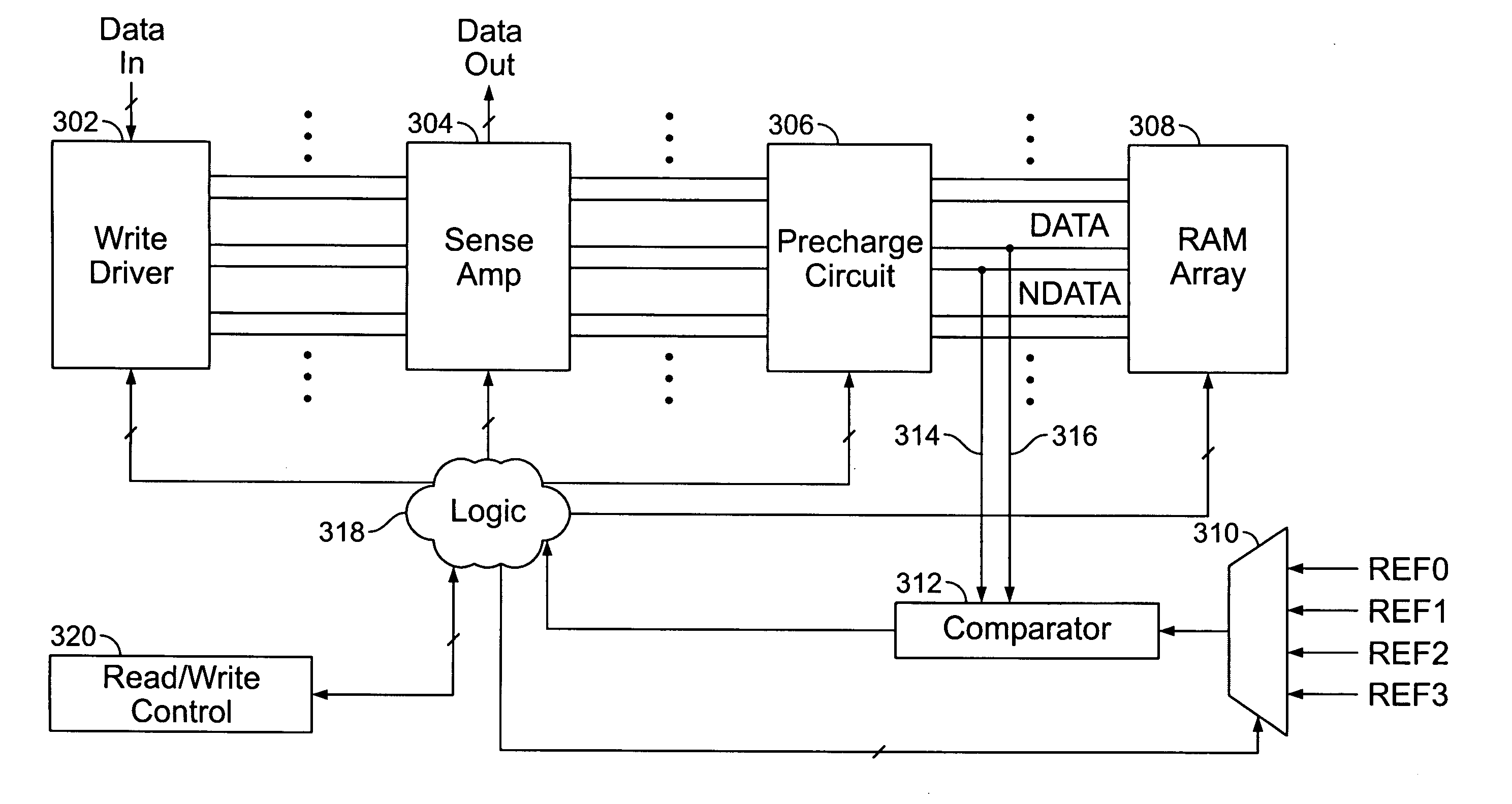
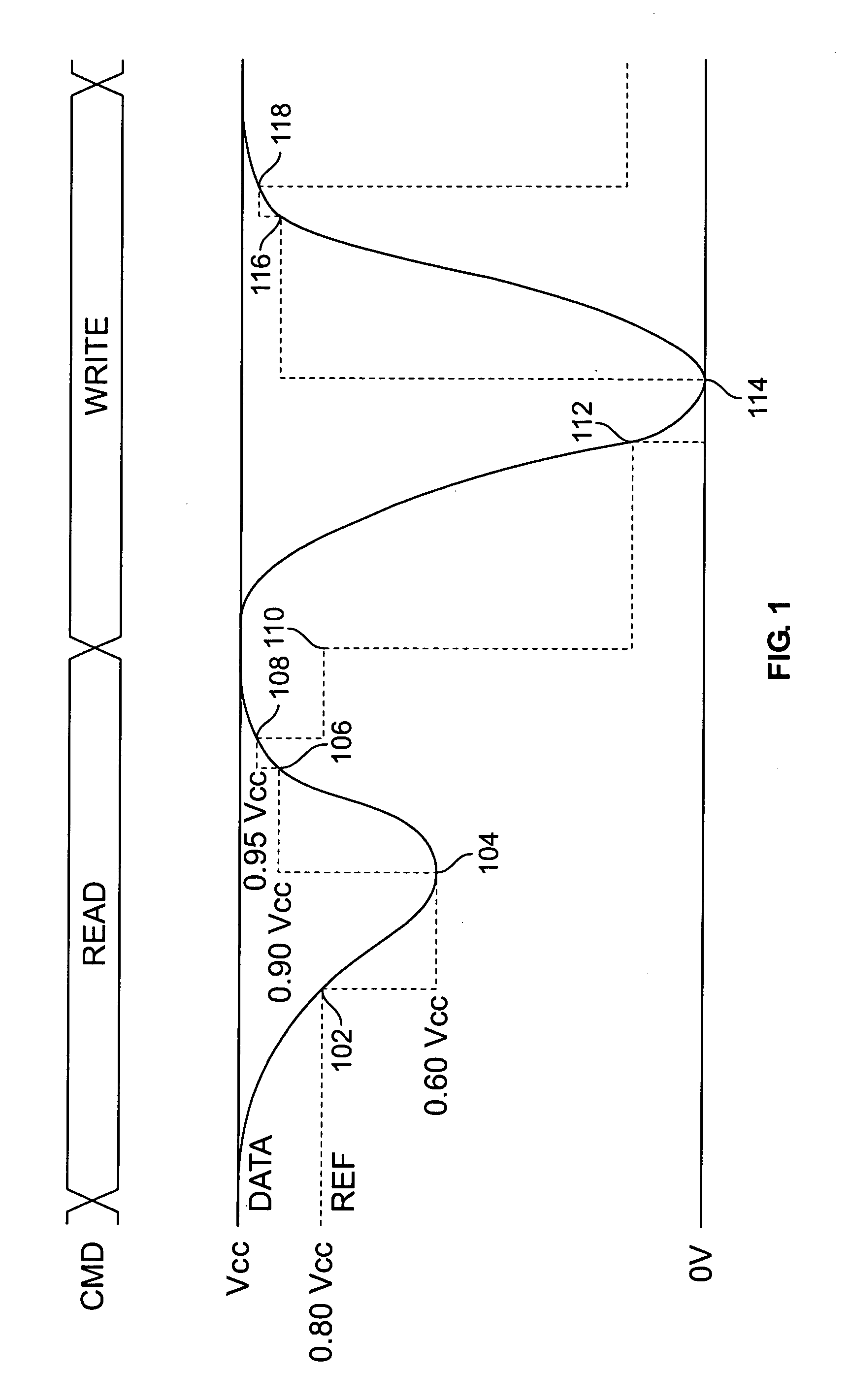
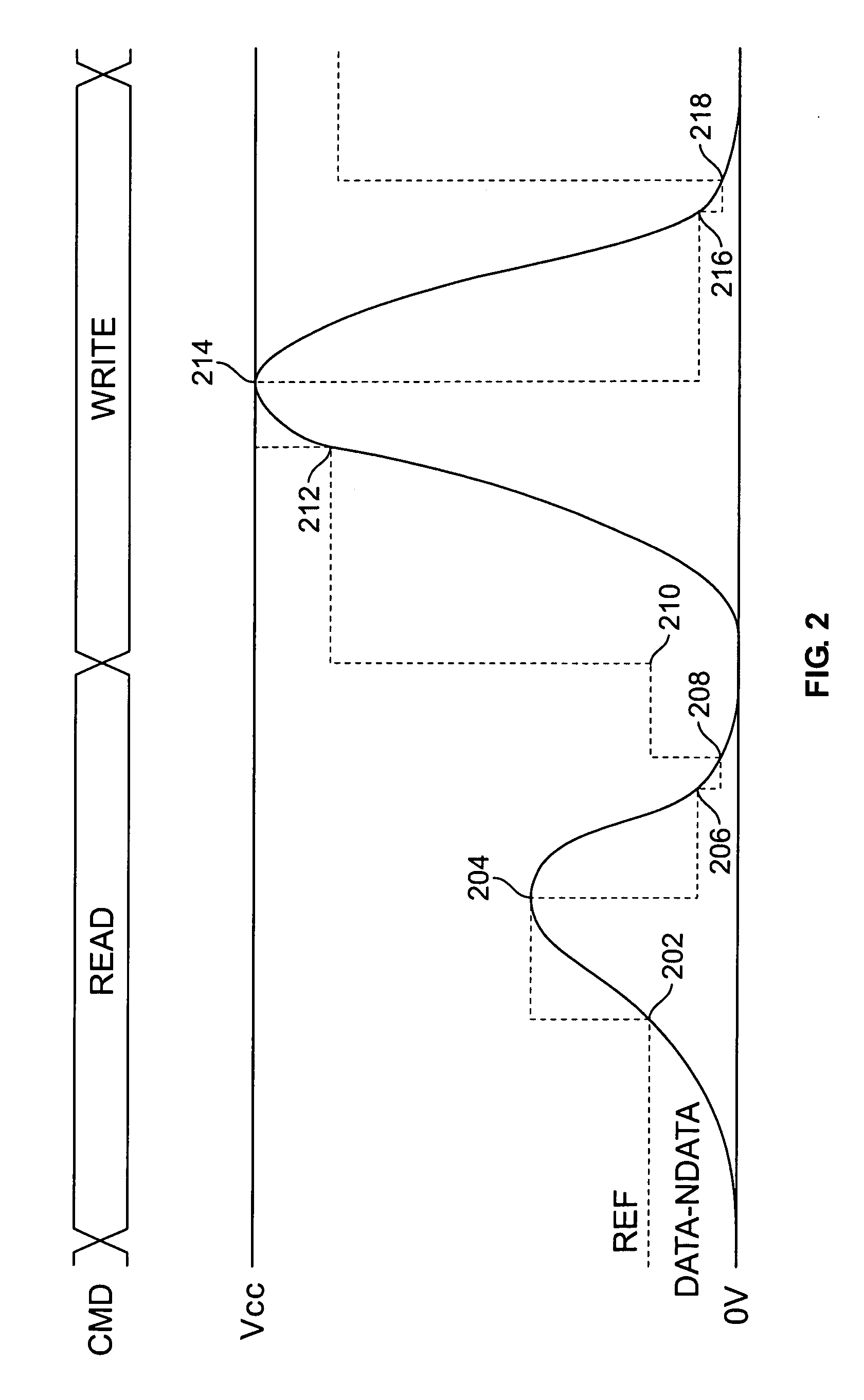
[0016]FIG. 1 is a timing diagram showing illustrative waveforms in accordance with the invention. Signal CMD encodes the operation being performed on the memory, if any. Signal DATA represents the voltage on a memory bit line, and signal REF represents a reference threshold voltage used for bit line control. In order to facilitate understanding of the invention, a brief description of exemplary memory operations is provided below.

[0017]Many memory systems use a pair of bit lines to transfer data to and from each cell. The bit lines in a given pair are referred to herein as DATA and NDATA. Before a read or write operation commences, both bit lines are precharged to a predetermined value by a precharge circuit. The embodiment described herein uses a precharge voltage of Vcc, though any suitable value, such as Vcc / 2 or 0V, could be used.

[0018]During a read operation, both bit lines are connected to the corresponding cell. Depending on the logical value stored in the cell, either DATA w...


PUM


Abstract

Circuitry and methods are provided for controlling memory operation by comparing bit line voltages to preset reference voltages. By relying on bit line voltage levels to determine when to start and end each stage of a read or write operation, reliance on precisely tuned delay chains is removed. Parasitic effects are automatically accounted for, as well as process, voltage, and temperature variations. This precise matching of operation timing to memory bit line conditions results in improved system performance.

Description

BACKGROUND OF THE INVENTION[0001]The control of memory bit lines, which are used to transfer data into and out of memory cells, is subject to precise timing constraints. For instance, a typical memory read operation includes driving bit lines by connecting them to the corresponding memory cells, amplifying the bit line voltages (e.g., with a sense amplifier), and precharging the bit lines in preparation for subsequent operations. Each of these stages must be triggered in sequence. If a particular stage is initiated too soon (e.g., the precharge stage is commenced before sense amplification has completed), data could be corrupted.[0002]A typical memory write operation has similar constraints. The operation often includes writing new data to bit lines using write drivers, connecting the bit lines to the corresponding memory cells, and precharging the bit lines in preparation for subsequent operations. As with read operations, the stages of a memory write must be triggered in the corre...

Claims


Application Information

Patent Timeline
Patent Type & Authority Patents(United States)
IPC IPC(8): G11C7/00
CPCG11C7/04G11C7/22G11C7/12G11C2207/2254
Inventor CHOE, KOK HENGKOK, EDWIN YEW FATTCHUA, KAR KENG
Owner ALTERA CORP
Why Eureka
Try Eureka