Method for producing III-IV group compound semiconductor layer, method for producing semiconductor light emitting element, and vapor phase growing apparatus

a technology of compound semiconductors and growing apparatuses, which is applied in the direction of crystal growth process, polycrystalline material growth, semiconductor lasers, etc., can solve the problems of crystallinity deterioration, crystallinity defects, and crystallinity deformation of algainp

Active Publication Date: 2006-05-23
XIAMEN SANAN OPTOELECTRONICS CO LTD
View PDF5 Cites 4 Cited by
  • Summary
  • Abstract
  • Description
  • Claims
  • Application Information

AI Technical Summary

Benefits of technology

[0031]According to one aspect of the present invention, there is provided a method for producing a III-V group compound semiconductor layer, comprising the steps of: forming a first III-V group compound semiconductor layer on a substrate in a reaction chamber; and supplying a III group material gas to the reaction chamber before or after the step of forming the first III-V group compound semiconductor layer to prevent re-evaporation of the III group gas in the reaction chamber.

Problems solved by technology

These may cause crystal defects.
However, through further research, the present inventors found that a phenomena which is not considered in the above conventional techniques is causing deterioration in crystallinity of AlGaInP.
Since InAs has a large lattice mismatch with GaAs,crystals are not grown normally.
Thus, crystal defects are generated.
Thus, crystals having good quality cannot be obtained.
Thus, crystal defects are generated at the growth interface.

Method used


Image

  • Method for producing III-IV group compound semiconductor layer, method for producing semiconductor light emitting element, and vapor phase growing apparatus
  • Method for producing III-IV group compound semiconductor layer, method for producing semiconductor light emitting element, and vapor phase growing apparatus
  • Method for producing III-IV group compound semiconductor layer, method for producing semiconductor light emitting element, and vapor phase growing apparatus

Examples


example 1

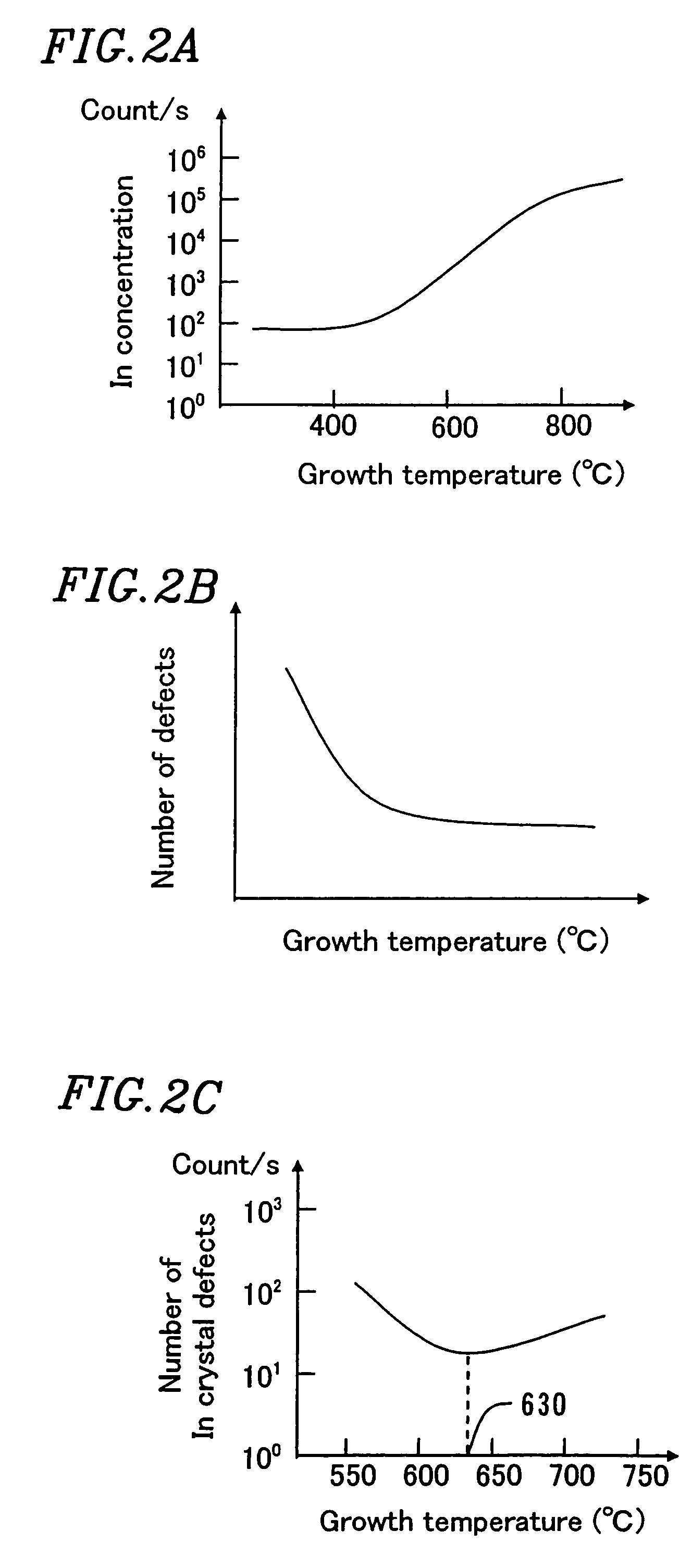
[0123]In Example 1, a GaAs buffer layer 12 is grown on a GaAs substrate 11 before a AlGaInP layer which forms a light-emitting portion 13 of a semiconductor light-emitting element is laminated, at a substrate temperature of 650° C., which is lower than the growth temperature for the AlGaInP layer, which forms the light-emitting portion 13, of 730° C.

[0124]FIG. 4 is a diagram showing a pattern in substrate temperature and material gas introduction during the growth over time in a method for producing a III-IV group compound semiconductor layer of Example 1.

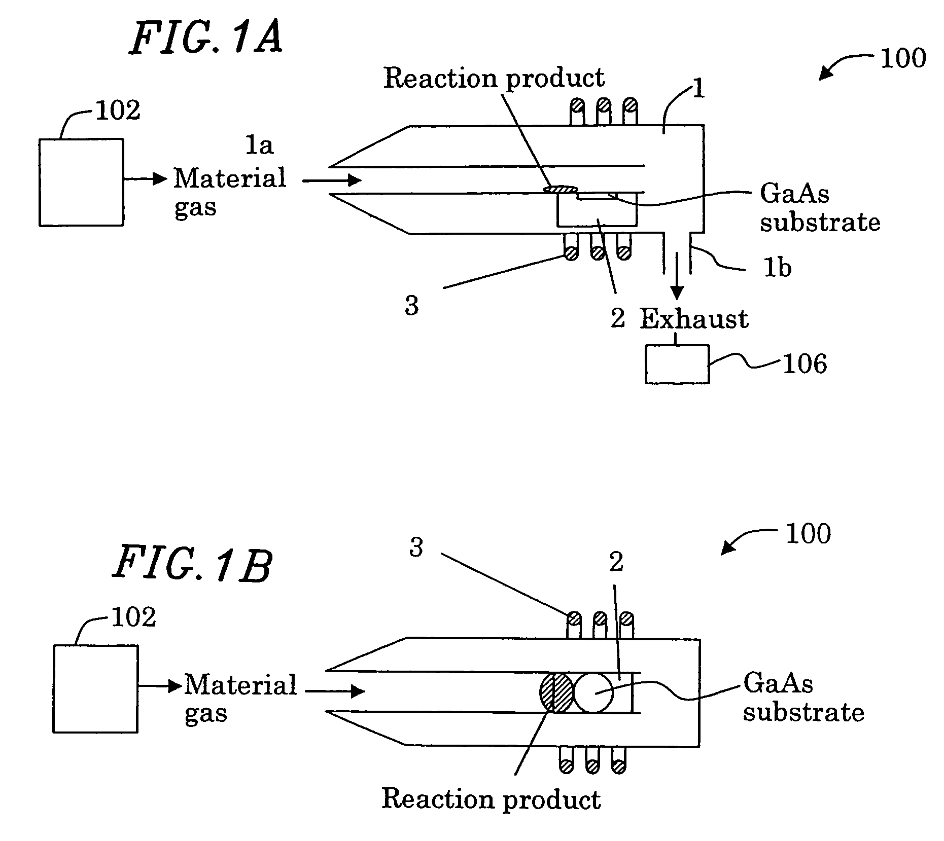
[0125]With reference to FIG. 4, first, a GaAs substrate 11 is placed on a substrate holding member 2 in a reaction chamber 1. The atmosphere in the reaction chamber 1 is reduced to desirable pressure. Then, as a V group material gas, AsH3 is introduced into the reaction chamber 1. Next, during a step of increasing substrate temperature of the GaAs substrate 11 to the growth temperature for the GaAs buffer layer 12 of 650° C., at th...

example 2

[0131]In Example 2, unlike in Example 1, a first GaAs buffer layer 12a is grown on a GaAs substrate 11 at 780° C., which is higher than the growth temperature for a AlGaInP layer, which forms a light-emitting portion 13, at 730° C., before a second GaAs buffer layer 12b is grown at 630° C., which is lower than the growth temperature for the AlGaInP layer, at 730° C. In Example 2, crystal growth of the GaAs buffer layer 12 is continued with a III group material gas being supplied during a temperature decreasing step before the second main GaAs buffer layer is formed. Though re-evaporated elements are generated, they are incorporated into crystals during the growth process and do not concentrate and accumulate on one interface. Thus, deterioration in the crystallinity can be suppressed.

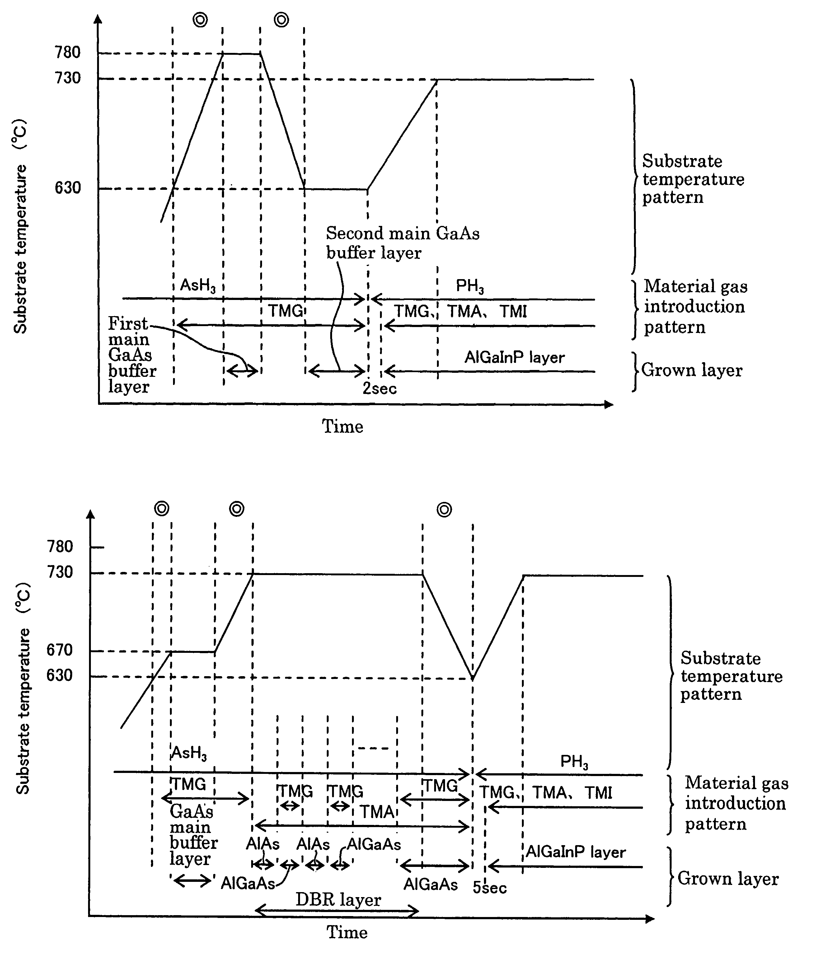
[0132]FIG. 5 is a diagram showing a pattern in substrate temperature and material gas introduction during the growth over time in a method for producing a III-IV group compound semiconductor layer of Ex...

example 3

[0140]In Example 3, as in Example 2, a first GaAs buffer layer 12a is grown on a GaAs substrate 11 at 780° C., which is higher than the growth temperature for a AlGaInP layer which forms a light-emitting portion 13, at 730° C., before a second GaAs buffer layer 12b is grown at 630° C., which is lower than the growth temperature for the AlGaInP layer, at 730° C.

[0141]FIG. 6 is a diagram showing a pattern in substrate temperature and material gas introduction during the growth over time in a method for producing a III-IV group compound semiconductor layer of Example 3.

[0142]With reference to FIG. 6, first, a GaAs substrate 11 is placed on a substrate holding member 2 in a reaction chamber 1. The atmosphere in the reaction chamber 1 is reduced to a desirable pressure. Then, as a V group material gas, AsH3 is introduced into the reaction chamber 1. Next, during a step of increasing substrate temperature of the GaAs substrate 11 to the growth temperature for the first GaAs buffer layer 1...


PUM

PropertyMeasurementUnit
temperatureaaaaaaaaaa

Abstract

A method for producing a III-V group compound semiconductor layer comprises the steps of: forming a first III-V group compound semiconductor layer on a substrate in a reaction chamber; and supplying a III group material gas to the reaction chamber before or after the step of forming the first III-V group compound semiconductor layer to prevent re-evaporation of the III group gas in the reaction chamber.

Description

BACKGROUND OF THE INVENTION[0001]1. Field of the Invention[0002]The present invention relates to a method for producing a III-IV group compound semiconductor layer, a method for producing a semiconductor light emitting element and a vapor phase growing apparatus.[0003]2. Description of the Related Art[0004]Conventionally, as a method for growing III-IV group compound semiconductor crystals having less crystal defects on a GaAs substrate, Japanese Laid-Open Publication No. 8-203837 describes a following method.[0005]FIG. 9 is a diagram showing a pattern in substrate temperature and material gas introduction during the growth over time in a conventional method for producing a III-IV group compound semiconductor layer disclosed in Japanese Laid-Open Publication No. 8-203837.[0006]First, a GaAs substrate is placed in a reaction container (reaction chamber). The atmosphere in the reaction container is reduced to desirable pressure. Then, as the V group material gas, AsH3 (arsine) is intr...

Claims


Application Information

Patent Timeline
Patent Type & Authority Patents(United States)
IPC IPC(8): H01L21/44C30B25/02C30B29/40H01L21/205H01L33/10H01L33/12H01L33/30H01S5/323
CPCC30B25/02C30B29/40H01L21/02395H01L21/02461H01L21/02463H01L21/0262H01L21/02507H01L21/02543H01L21/02576H01L21/02579H01L21/02502
Inventor NAKAMURA, JUNICHISASAKI, KAZUAKI
Owner XIAMEN SANAN OPTOELECTRONICS CO LTD
Why Eureka
Try Eureka