High latency timing circuit

a timing circuit and high latency technology, applied in the field of timing circuits, can solve the problems of reducing the stability of the overall circuit, circuits tend to become unstable, loops with high latency, time delay, etc., and achieve the effect of reducing latency and high speed

Inactive Publication Date: 2006-05-23
MARVELL ASIA PTE LTD
View PDF22 Cites 2 Cited by
  • Summary
  • Abstract
  • Description
  • Claims
  • Application Information

AI Technical Summary

Benefits of technology

[0008]The present invention is intended to overcome the drawbacks noted above and provides a high speed timing recovery system with reduced latency.
[0010]In another aspect, the invention provides a phase locked loop circuit, including a digital filter loop for timing recovery. The circuit includes a phase synchronization feedback loop, a frequency synchronization feedback loop, and a phase shift measurement circuit. The phase shift measurement circuit includes a shift register. When an input to the frequency synchronization feedback loop is set to zero, the phase synchronization feedback loop is operated at a high bandwidth rate to synchronize phase and to compute a value of frequency offset using the shift register. Once the frequency offset has been computed, the input to the frequency synchronization feedback loop is set to the computed value of frequency offset, and the frequency synchronization feedback loop and the phase synchronization feedback loop are jointly operated at a low bandwidth rate to synchronize frequency and to track further deviations of phase or frequency. The use of a low bandwidth rate ensures circuit stability.
[0013]In still another aspect, a digital data acquisition loop is used with a phase shift measurement circuit. The loop includes a phase timing circuit having an overflow output, including a control signal. The control signal is provided to the phase shift measurement circuit, which outputs a frequency offset corresponding to the overflow output. The loop also includes a frequency timing circuit, which receives the frequency offset from the phase shift measurement circuit and adjusts the frequency timing of an input data stream based on the received frequency offset. The loop may also initially disable the frequency timing circuit during an acquisition period corresponding to the outputting of the frequency offset, and subsequently enable the frequency timing circuit during a tracking period that follows the outputting of the frequency offset. The loop may operate at a high speed during the acquisition period to ensure high performance, and at a low speed during the tracking period to ensure loop stability.
[0020]In another aspect of the invention, a method of controlling frequency and phase in a high-speed control circuit includes the steps of executing an acquisition mode in which phase deviation is corrected and frequency deviation is computed, and executing a tracking mode in which frequency deviation is corrected. The acquisition mode operates at a high bandwidth value to cause the high-speed control circuit to operate at a high speed related to the high bandwidth value. The tracking mode operates at a low bandwidth value to maintain stability of the circuit.

Problems solved by technology

However, the joint use of the two feedback loops reduces the stability of the overall circuit, as compared to the stability of each individual feedback loop.
In other words, if the circuit is operated at a sufficiently low speed, the circuit remains stable, but as the operation speed increases, the circuit tends to become unstable.
This causes the loop to have a high latency, or time delay, associated with it.
A high latency generally causes degraded performance of the timing loop, which in turn requires that the loop bandwidth be reduced in order to maintain loop stability.
Thus, a dilemma for implementation of high speed channels is presented.

Method used


Image

  • High latency timing circuit
  • High latency timing circuit
  • High latency timing circuit

Examples


Embodiment Construction

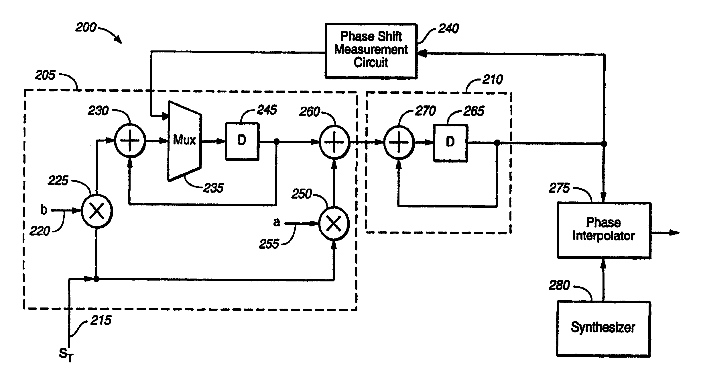
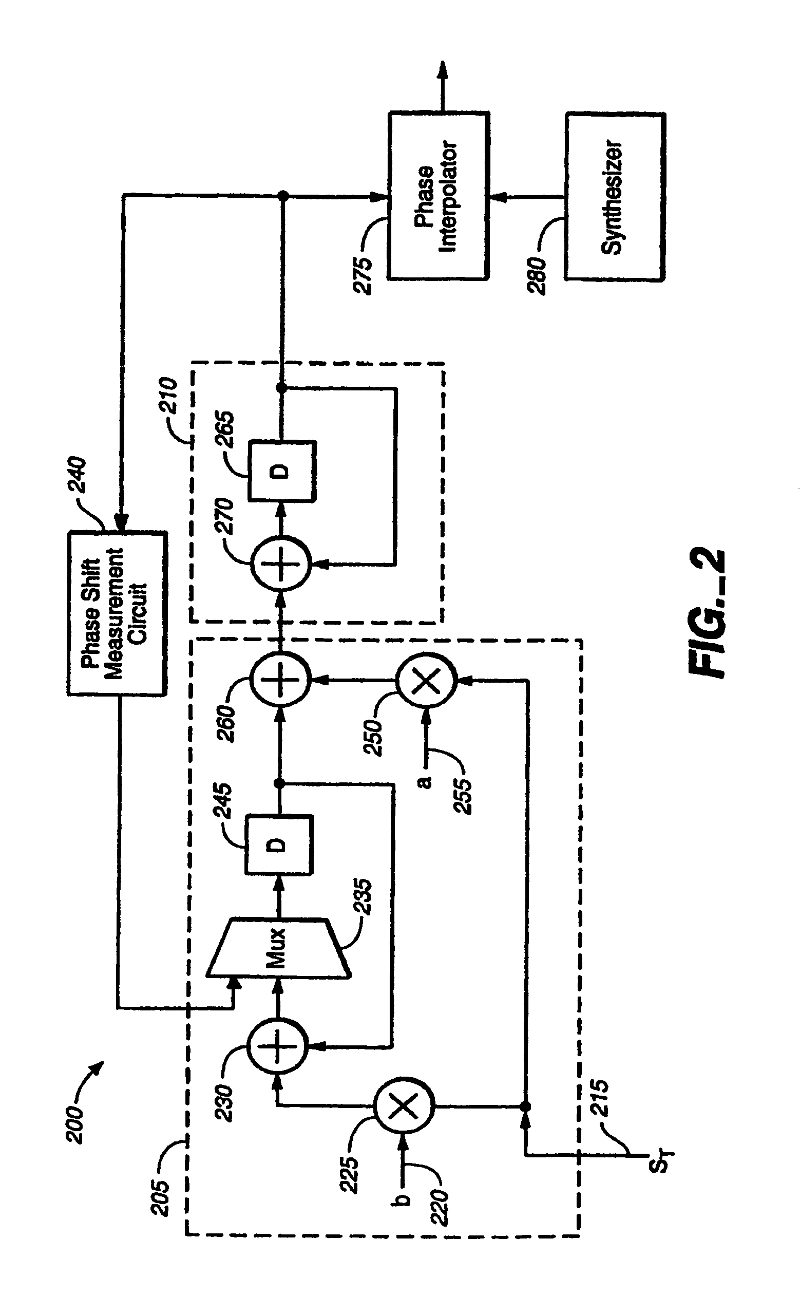
[0029]The present invention addresses the need for more effective timing recovery circuits to be used in high-speed channels, such as a read channel of a hard disk drive. In the development of the present invention, the inventor has recognized that a timing circuit (e.g., a phase-locked loop circuit) can be viewed as being either a type I timing circuit, in which only phase correction occurs, or a type II timing circuit, in which both phase correction and frequency correction occur. In a type I circuit, because only phase correction occurs, the frequency integration feedback loop need not be operational. Thus, in a type I circuit, a higher loop bandwidth and correspondingly higher speed are possible, as compared to a type II circuit having the same latency, because a type I circuit is inherently more stable than a type II circuit.

[0030]A type II timing circuit can be used as a type I timing circuit by disabling the frequency integration feedback loop. This may be achieved by setting...


PUM


Abstract

A phase locked loop circuit includes a frequency integrator responsive to a received signal. A phase integrator is responsive to the frequency integrator and a phase shift measurement circuit is responsive to the phase integrator and in communication with the frequency integrator. The phase shift measurement circuit is configured to supply a frequency offset to an input of the frequency integrator. When the input to the frequency integrator selectively receives a predetermined value, the phase integrator is configured to synchronize phase and to output a phase signal, and the phase shift measurement circuit is configured to determine the frequency offset using the phase signal. When the input to the frequency integrator circuit selectively receives the determined frequency offset, the frequency integrator circuit and the phase integrator are configured to track deviations of frequency and phase in the received signal and to adjust frequency and phase of the received signal.

Description

CROSS-REFERENCE TO RELATED APPLICATIONS[0001]This application is a continuation of U.S. patent application Ser. No. 09 / 725,818 filed on Nov. 30, 2000. The disclosure of the above application is incorporated herein by reference.BACKGROUND OF THE INVENTION[0002]1. Field of the Invention[0003]The present invention relates to a timing circuit for synchronization of phase and frequency, and particularly to such a circuit having a highly pipelined structure, thereby optimizing the circuit for use in a high-speed read channel while inducing high latency.[0004]2. Description of the Related Art[0005]A clock and data recovery system, which may be referred to as a channel, invariably requires a timing recovery feedback loop for clock synchronization. Historically, this need has been fulfilled through the use of a phase-locked loop timing circuit. Phase-locked loop timing circuits typically include a frequency integration feedback loop and a phase integration feedback loop. They operate by firs...

Claims


Application Information

Patent Timeline
Patent Type & Authority Patents(United States)
IPC IPC(8): H03L7/00G06F1/12H03L7/099H03L7/107H03L7/113H04L7/00H04L7/033
CPCH03L7/107H03L7/1075H03L7/0994H03L7/113H04L7/0004H04L7/0331
Inventor SUTARDJA, PANTAS
Owner MARVELL ASIA PTE LTD
Why Eureka
Try Eureka