Single and multi layer variable voltage protection devices and method of making same

a protection device and variable voltage technology, applied in the field of variable voltage protection devices, can solve the problems of high current and voltage, damage to electrical devices, transmission loss, etc., and achieve the effect of superior performan

Inactive Publication Date: 2006-05-23
SURGX CORP
View PDF11 Cites 67 Cited by
  • Summary
  • Abstract
  • Description
  • Claims
  • Application Information

AI Technical Summary

Benefits of technology

[0009]In another aspect of the present invention, it has been found that superior performance can be provided by a variable voltage protection component which comprises the combination of (a) a layer of variable voltage protection material comprising a binder containing conductive particles and / or semiconductive particles; and (b) a layer of neat dielectric polymer or glass in contact with one surface of said layer of variable voltage material; wherein the neat dielectric polymer or glass layer is present in a thickness of less than about 1.6 mils. It has been found that the presence of the thin layer of neat dielectric polymer or glass on the surface of the binder / particle type of variable voltage protection material provides a component having desirable voltage clamping properties, as well as other desirable properties.
[0010]In another aspect, this invention provides a layered variable voltage protection component comprising a first layer of variable voltage protection material comprising a binder having dispersed therein at least about 20% by volume of conductive or semiconductive particles; a second layer of variable voltage protection material in contact with the first layer comprising a binder having dispersed therein at least 40% by volume of conductive or semiconductive particles; and a third layer of variable voltage protection material in contact with said second layer comprising a binder having dispersed therein at least 20% by volume of conductive or semiconductive particles. It has been found that the multiple layer construction provides an opportunity to vary the conductor particle loading and / or semiconductor particle loading in each layer, such that the outer layers contain lower particle loadings than the inner layer, in order to achieve a wide range of clamping voltages and other desired properties. In an additional aspect of this invention, it has been found that the outer layer in contact with the electrical conductor of the electronic device should have a lower particle loading than the inner layer with a higher particle loading, but in such case the other outer layer in contact with the ground plane can be higher or lower in particle loading. In an additional aspect of this invention, this multi-layer variable voltage protection component can further be provided with a thin layer of the neat dielectric polymer or glass as referred to above on one outside surface or both outside surfaces, in order to provide additional properties and characteristics of the component. In this aspect of the invention, the layer on the side of the electrical conductor can have a higher or lower particle loading than the inner layer provided the neat dielectric polymer or glass layer is positioned between the outer layer and the electrical conductor. In another aspect of this invention this multiple layer component can be provided with a conductive, e.g., metal, layer interposed between the first layer and second layer and / or between the second layer and third layer of variable voltage protection material. In yet another aspect of this invention, these multiple layer components themselves can be stacked, with or without the outer layers of neat dielectric polymer or glass layers, and with or without an intervening layer of neat dielectric polymer or glass between components to achieve desired performance characteristics.

Problems solved by technology

Voltage transients can induce very high currents and voltages that can penetrate electrical devices and damage them, either causing hardware damage, such as semiconductor burnout, or electronic upset, such as transmission loss or loss of stored data.
Such strikes can suddenly overload a system's electronics.

Method used


Image

  • Single and multi layer variable voltage protection devices and method of making same
  • Single and multi layer variable voltage protection devices and method of making same

Examples


Embodiment Construction

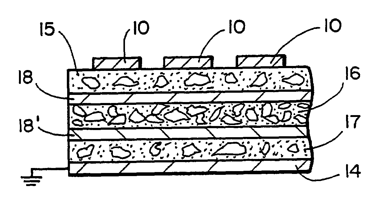
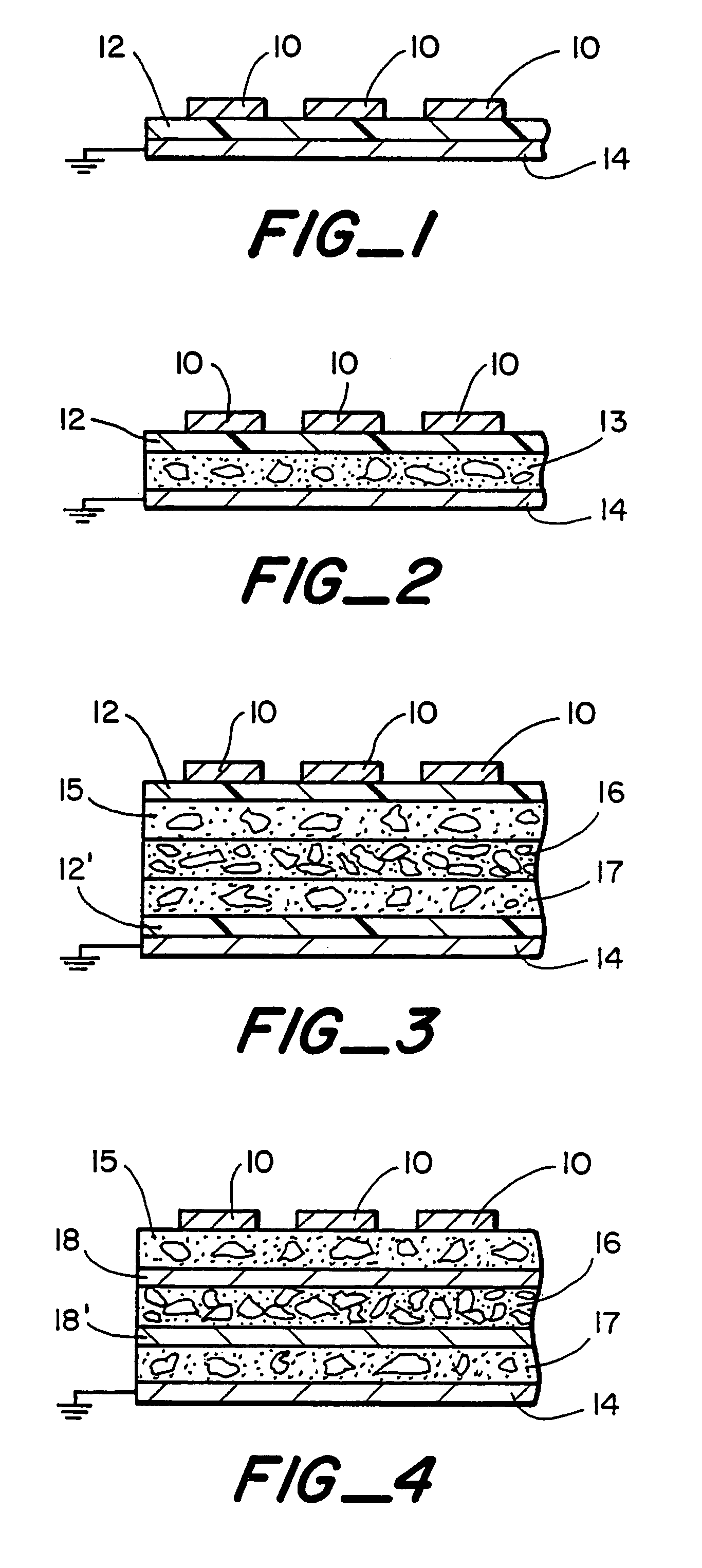
[0016]Referring to the first aspect of this invention which comprises a variable voltage protection device comprising as the variable voltage protection material a thin layer of a neat dielectric polymer or glass, it has been found that such a device is surprisingly effective at a desired range of clamping voltages provided that the layer of neat dielectric polymer or glass is sufficiently thin. It has been found that for some polymers a layer of less than about 0.8 mil will provide effective overvoltage protection under various conditions, while for other polymers a layer of less than about 1.6 mils provides the desired performance characteristics. It is preferable in many variable voltage protection applications that the polymer layer be less than about 0.5 mil and more preferably less than about 0.2 mil. Similarly, when the layer is a glass it is preferred that the layer be less than about 0.8 mil, but for some glasses in certain applications a thickness of up to about 3.8 mils i...


PUM


Abstract

Disclosed is a variable voltage protection device for electronic devices which in one aspect comprises a thin layer of neat dielectric polymer or glass positioned between a ground plane and an electrical conductor for overvoltage protection, wherein the neat polymer or glass layer does not include the presence of conductive or semiconductive particles. Also disclosed is the combination of the neat dielectric polymer or glass thin layer positioned on a conventional variable voltage protection material comprising a binder containing conductive or semiconductive particles. A multi-layer variable voltage protection component is disclosed comprising three layers of overvoltage protection material wherein the outer two layers contain a lower percentage of conductive or semiconductive particles and wherein the inner layer contains a higher percentage of conductive or semiconductive particles. The multi-layer component can optionally be used in combination with the neat dielectric polymer or glass layer and can optionally have interposed metal layers. A method is disclosed for dispersing insulative particles and conductive or semiconductive particles in a binder using a volatile solvent for dispersement of the insulative particles and the conductive or semiconductive particles before mixing with the binder.

Description

[0001]This is a continuation of application Ser. No. 09 / 139,306 filed Aug. 24, 1998, now U.S. Pat. No. 6,162,159.FIELD OF THE INVENTION[0002]The present invention relates generally to variable voltage protection devices used to protect electronic circuits from overvoltage transients caused by lightning, electromagnetic pulses, electrostatic discharges, ground loop induced transients, or inductive power surges. The present invention relates particularly to materials of construction for variable voltage protection components and methods of making variable voltage protection components and devices.BACKGROUND OF THE INVENTION[0003]Voltage transients can induce very high currents and voltages that can penetrate electrical devices and damage them, either causing hardware damage, such as semiconductor burnout, or electronic upset, such as transmission loss or loss of stored data. The voltage transients produce large voltage spikes with high peak currents (i.e, overvoltage). The three basic...

Claims


Application Information

Patent Timeline
Patent Type & Authority Patents(United States)
IPC IPC(8): H01C7/10G07B1/00G07B5/02
CPCG07B5/02G07B1/00
Inventor SHRIER, KAREN P.BEHLING, GERALD R.INTRATER, JAMES B.JOSHI, KAILASH C.ALSTON, JR., WILLIAM W.
Owner SURGX CORP
Why Eureka
Try Eureka