
Component carrier

a carrier and component technology, applied in the field of filters, can solve the problems of requiring extensive repair and/or replacement at great cost, straying electrical energy, and reducing the service life of electronic equipment, so as to eliminate the susceptibility to over voltage and emissions, and low cost

Inactive Publication Date: 2006-05-23
X2Y ATTENUATORS L L C
View PDF469 Cites 53 Cited by
  • Summary
  • Abstract
  • Description
  • Claims
  • Application Information

AI Technical Summary

Benefits of technology

[0013]Based upon the foregoing and because of the sensitive nature of electronic technology there is also a need for combining electromagnetic filtering with surge protection to eliminate the susceptibility to over voltages and emissions from external sources. Due to the highly competitive nature of today's electronic industry such a differential and common mode filter / surge protector must be inexpensive, miniaturized, low in cost and highly integrated to be incorporated into a plurality of electronic products.
[0014]It is therefore a main object of the invention to provide an easily manufactured and adaptable multi-functional electronic component which filters electromagnetic emissions caused by differential and common mode currents.
[0015]It is another object of the invention to provide a protective circuit arrangement which may be mass produced and adaptable to include one or more protective circuits in one component package to provide protection against voltage transients, over voltages and electromagnetic interference.

Problems solved by technology

The majority of electronic equipment produced presently, and in particular computers, communication systems, military surveillance equipment, stereo and home entertainment equipment, televisions and other appliances include miniaturized components to perform new high speed functions and electrical interconnections which according to the materials from which they are made or their mere size are very susceptible to stray electrical energy created by electromagnetic interference or voltage transients occurring on electrical lines.
Voltage transients can severely damage or destroy such micro-electronic components or contacts thereby rendering the electronic equipment inoperative, and requiring extensive repair and / or replacement at great cost.
Electrical interference in the form of EMI or RFI can be induced into electrical lines from such sources as radio broadcast antennas or other electromagnetic wave generators.
Transient voltages occurring on electrical lines can be induced by lightning which produces extremely large potentials in a very short time.
In a similar manner, nuclear electromagnetic pulses (EMP) generate even larger voltage spikes with faster rise time pulses over a broad frequency range which is detrimental to most electronic devices.
Other sources of large voltage transients are found to be associated with voltage surges occurring upon the switching off or on of some electronic power equipment as well as ground loop interference caused by varying ground potentials.
Existing protection devices, primarily due to their architecture and basic materials, do not provide adequate protection in a single integrated package.
While the above referenced electronic components accomplish their respective tasks, usage of such components has been limited for a number of reasons.
First, the number of such components required continues to increase as applications, such as data buses, continue to grow.
Second, by their nature the electronic components referred to are delicate structures which do not handle physical stress well.
During the manufacture of electronic products a number of mechanical stresses associated with handling and soldering can damage the components.
Another drawback to using the referenced electronic components is that it becomes very tedious to manually handle and mount the components on electronic products being assembled.
This often time translates into lower product yields and added expense due to broken or misconnected components.
A further disadvantage to some of the components is that they include leads for thru-hole insertion.
Physical stressing, bending or applying torque to the leads can cause a failure in the final product, either immediately or later thereby affecting the products overall reliability.

Method used


Image

  • Component carrier
  • Component carrier
  • Component carrier

Examples


Embodiment Construction

[0064]Specific types of surface mount components such as differential and common mode filters as are disclosed in application Ser. No. 09 / 008,769, now U.S. Pat. No. 6,097,581, which is a continuation-in-part of application Ser. No. 08 / 841,940, now U.S. Pat. No. 5,909,350, both of which are incorporated herein by reference.

[0065]Due to the continued and increasing use of electronics in daily life and the amount of electromagnetic interference (EMI) and emissions generated, new world electromagnetic compatibility (EMC) requirements are being specified daily for use in such diverse applications as in the home, hospitals, automotive, aircraft and satellite industries. The present invention is directed towards a physical architecture for an electronic component which provides EMI suppression, broad band I / O-line filtering, EMI decoupling noise reduction and surge protection in one assembly.

[0066]To propagate electromagnetic energy two fields are required, an electric and magnetic. Electr...


PUM


Abstract

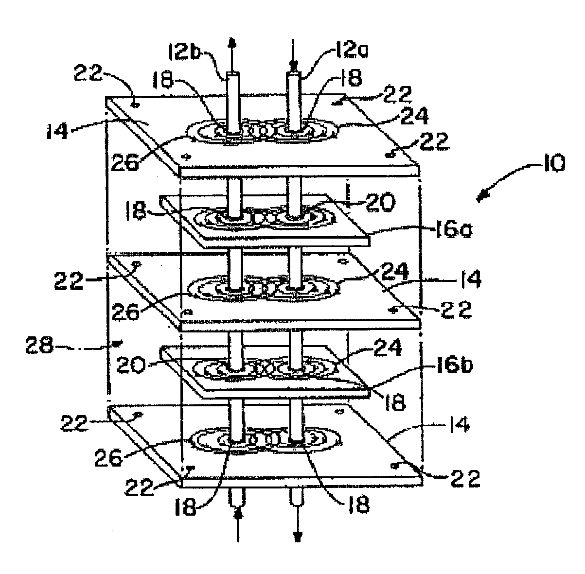
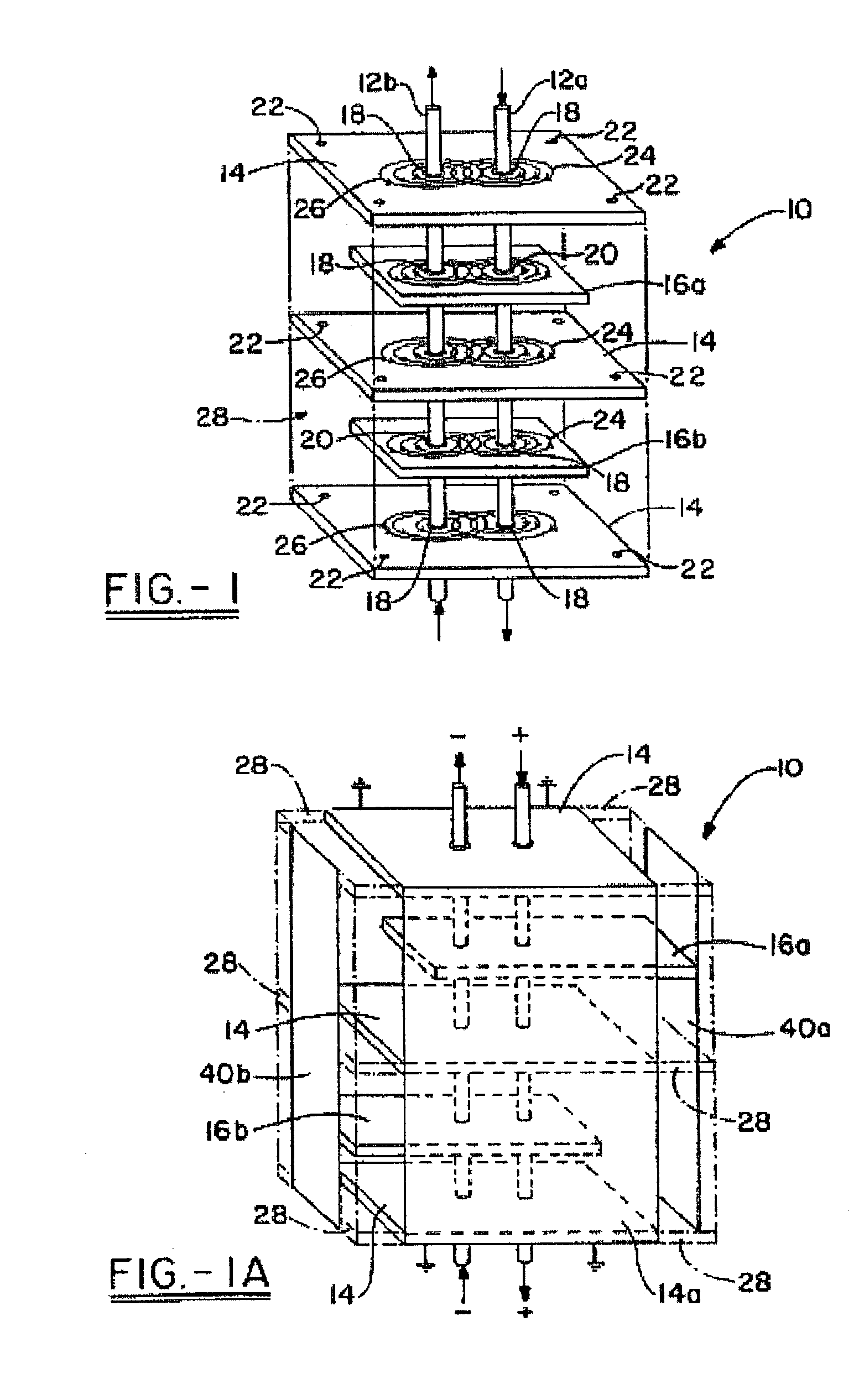
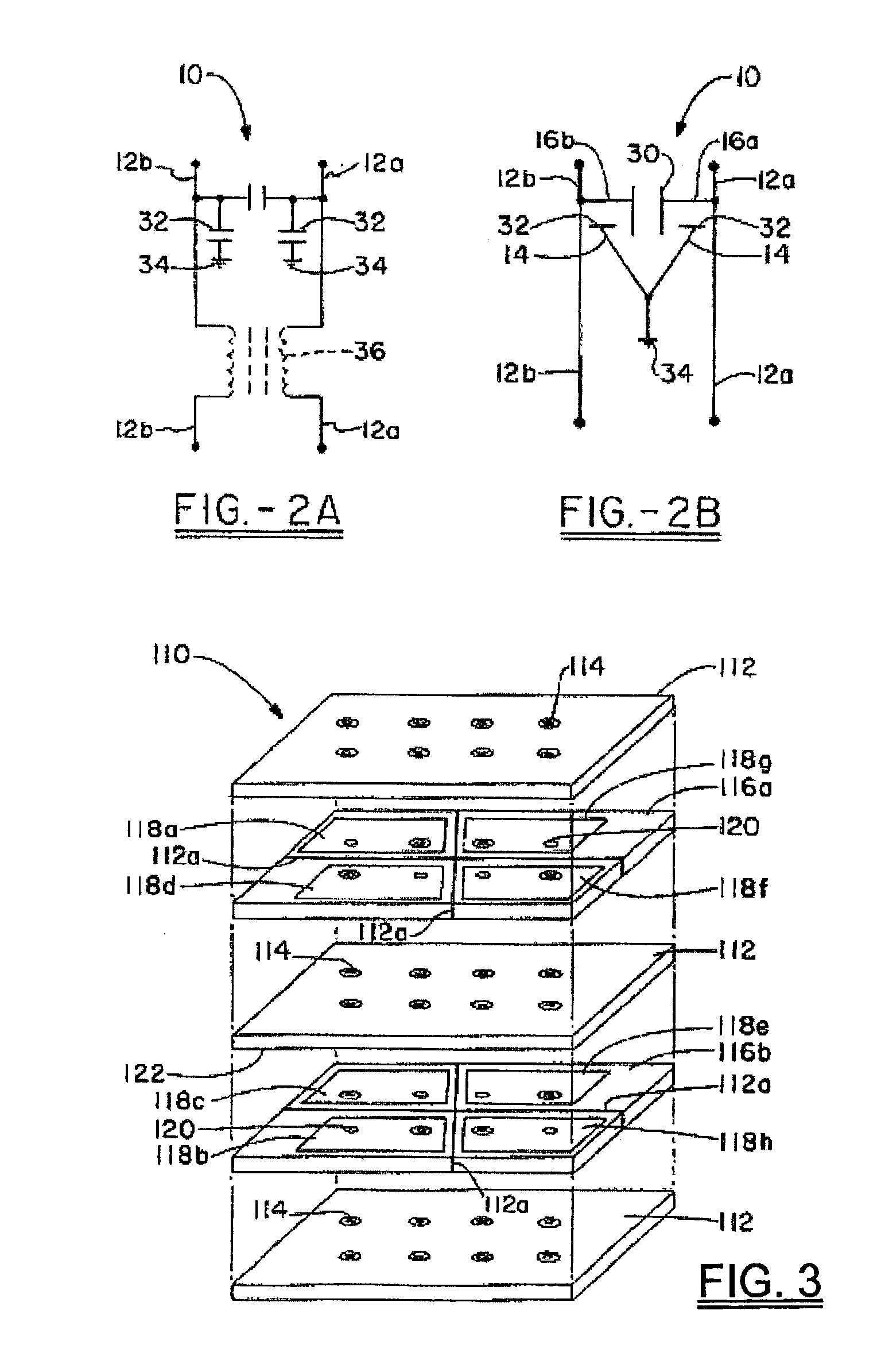
The present invention is a surface mount component carrier comprised of a disk of insulating material having at least two apertures. The disk is substantially covered by a metalized ground surface and includes at least two conductive pads surrounding the apertures, and insulating bands which surround each conductive pad. The insulating bands separate and electrically isolates the conductive pads from the metalized ground surface. A surface mount component, such as a differential and common mode filter, is positioned lengthwise between the two conductive pads and operably coupled to the carrier. Once the surface mount component is coupled to the carrier, the combination can be manipulated, either manually or through various types of automated equipment, without subjecting the surface mount component to mechanical and physical stresses normally associated with the handling of miniature components. The carrier also provides the added benefit of improved shielding from electromagnetic interference and over voltage dissipation due to the surface area of the metalized ground surface. The same concept for the above described carrier is also incorporated into several alternate embodiments, either independently or embedded within electronic connectors.

Description

[0001]This application is a continuation of application Ser. No. 09 / 945,329 filed Aug. 31, 2001 now U.S. Pat. No. 6,650,525, which is a continuation of application Ser. No. 09 / 697,484 filed Oct. 26, 2000 now abandoned, which is a continuation of both application Ser. No. 09 / 056,436 filed Apr. 7, 1998, now abandoned, and application Ser. No. 09 / 056,379 filed Apr. 7, 1998, now U.S. Pat. No. 6,018,448, which is a continuation-in-part of application Ser. No. 09 / 008,769 filed Jan. 19, 1998, now U.S. Pat. No. 6,097,581, which is a continuation-in-part of application Ser. No. 08 / 841,940 filed Apr. 8, 1997, now U.S. Pat. No. 5,909,350. The disclosures of the foregoing applications are all incorporated herein by reference.TECHNICAL FIELD[0002]The present invention relates to a filter for protecting electronic circuitry from electromagnetic field interference (EMI), over voltages and preventing electromagnetic emissions. More specifically, this invention relates to a multi-functional electron...

Claims


Application Information

Patent Timeline
IPC IPC(8): H02H1/00H01R13/719H03H1/00H05K1/02H05K1/14H05K1/16H05K1/18H05K3/34
CPCH01G4/012H01R13/719H01G4/30H01G4/35H05K3/3436H05K1/141H05K1/162H05K1/18H05K1/181H05K1/0237
Inventor ANTHONY, ANTHONY A.
Owner X2Y ATTENUATORS L L C
Learn More