Supercharge Your Innovation With Domain-Expert AI Agents!

Thin-film transistor and method of manufacture thereof

Inactive Publication Date: 2006-05-30
NEC LCD TECH CORP
View PDF45 Cites 10 Cited by
  • Summary
  • Abstract
  • Description
  • Claims
  • Application Information

AI Technical Summary

Benefits of technology

[0019]In addition, an amorphous material is formed as an amorphous layer, and thereafter, a laser beam may be irradiated on the amorphous material to form a gate electrode having a crystalline layer formed on the surface of the amorphous material. By forming the gate electrode in this manner, drawbacks caused by channeling of ions can be suppressed.
[0021]In addition, annealing at not lower than 300° C. is performed after the silicon thin film is formed, and thereafter a hydrogen introducing process is performed, so that the surface of the silicon thin film can be protected.

Problems solved by technology

For this reason, in the active matrix LCD, in accordance with a reduction in size or an increase in resolution, a connection pitch between the substrate and the peripheral driver integrated circuit decreases, and the connection cannot be easily achieved.
However, since the polycrystalline silicon TFT is manufactured by the high-temperature process of about 1,000° C. as described above, an inexpensive low-melting-point glass substrate which can be used in an active matrix LCD cannot be used, and an expensive quartz substrate is inevitably used.
That is, a liquid crystal display using an inexpensive low-melting-point glass substrate and a polycrystalline silicon TFT cannot be easily formed.
In this manner, although it is possible to use a low-melting-point glass substrate, a new problem is posed.
More specifically, a heat treatment temperature for a gate insulating film must be decreased with a decrease in process temperature of the entire manufacturing process, and the quality of the gate insulating film is deteriorated.
In this manner, the gate insulating film and the gate electrode (Al) easily react to each other and therefore, if a reduction in thickness of a gate insulating film is achieved with a reduction in TFT element size and with a reduction in drive voltage, the reliability of the gate insulating film is considerably deteriorated.
More specifically, the ions are penetrated through the gate electrode to reach the inner side of the gate insulating film or the inner side of the crystallized silicon thin film, and the transistor characteristics may be deteriorated.

Method used


Image

  • Thin-film transistor and method of manufacture thereof
  • Thin-film transistor and method of manufacture thereof
  • Thin-film transistor and method of manufacture thereof

Examples


first embodiment

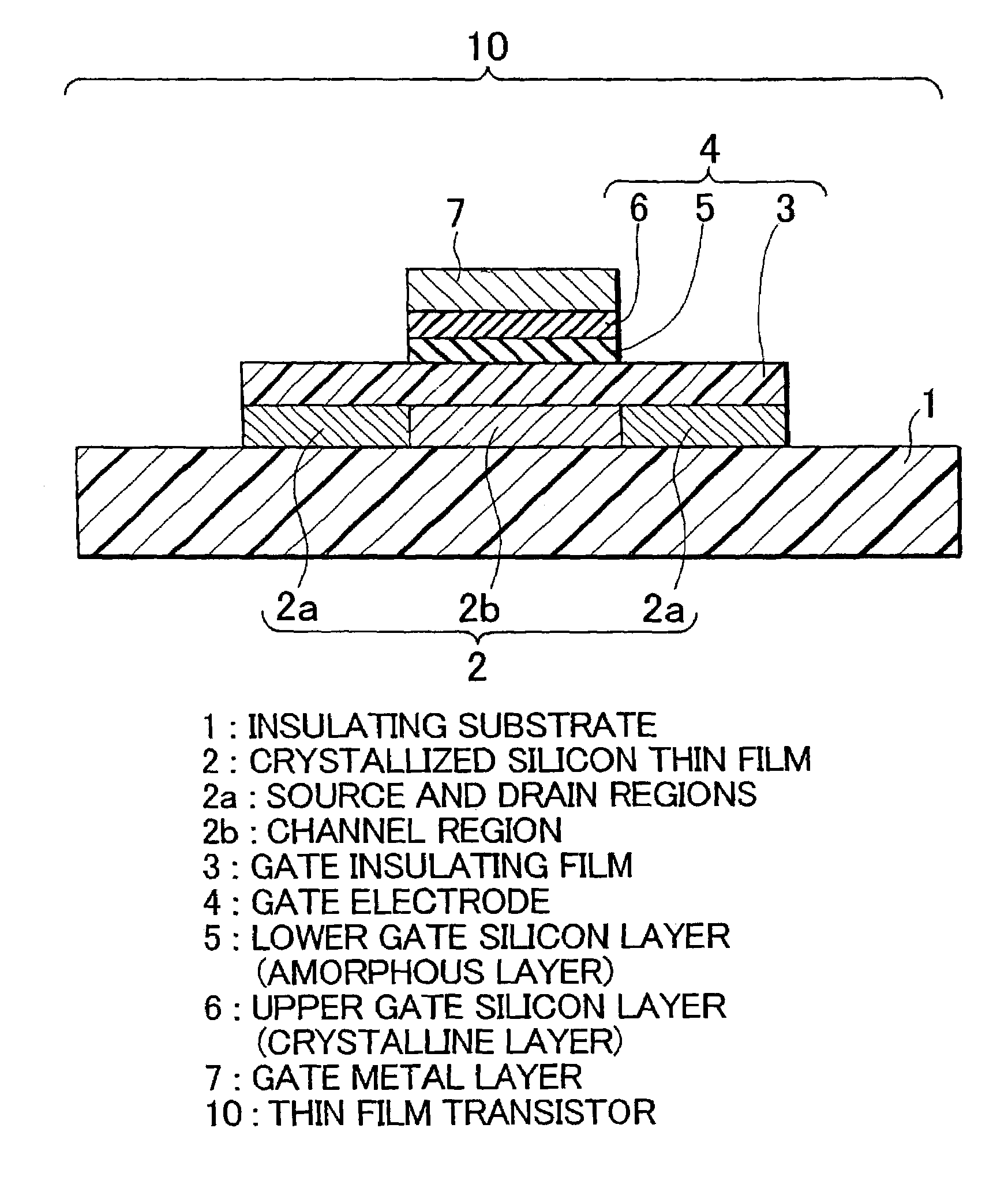
[0038]the present invention will be described below with reference to FIG. 1. Reference numeral 10 shown in FIG. 1 denotes a thin film transistor.

[0039]The thin film transistor 10 comprises a crystallized silicon thin film 2 having source and drain regions 2a and a channel region 2b formed on an insulating substrate 1 as shown in FIG. 1, a gate insulating film 3 formed on the crystallized silicon thin film 2 and constituted by, e.g., a silicon oxide film, and a gate electrode 4 formed on the gate insulating film 3.

[0040]In this case, as the insulating substrate 1, a glass substrate is used. In addition, the crystallized silicon thin film 2 is formed by a non-doped (impurity-undoped) film, and the source and drain regions 2a are formed such that impurity ions such as phosphorous ions, boron ions or arsenic ions are implanted or introduced at a high-concentration by using an ion implantation method or an ion doping method to control valence electrons.

[0041]The gate electrode 4 compris...

second embodiment

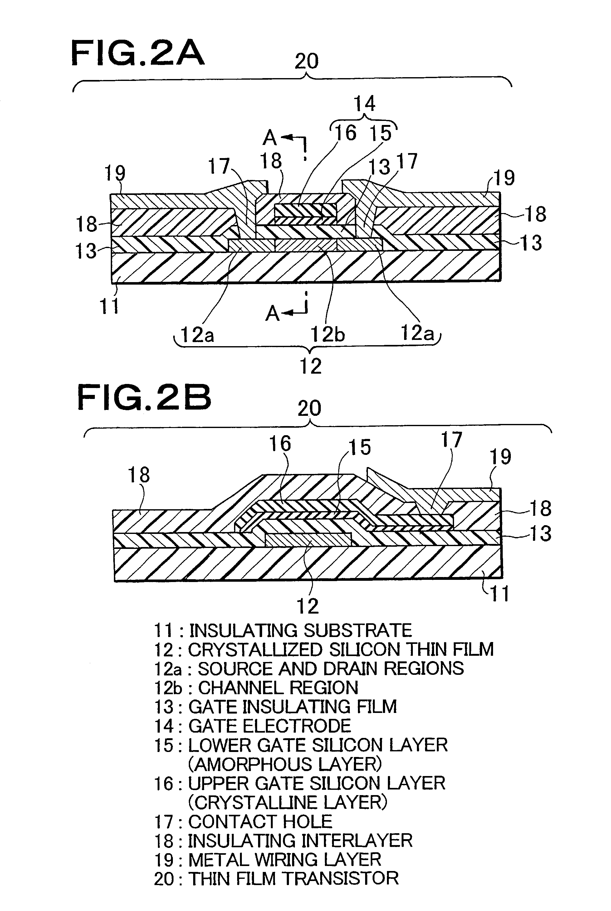
[0044]the present invention will be described below with reference to FIGS. 2A and 2B. Reference numeral 20 shown in FIGS. 2A and 2B denotes a thin film transistor.

[0045]The thin film transistor 20 comprises a crystallized silicon thin film 12 having source and drain regions 12a and a channel region 12b formed on an insulating substrate 11 as shown in FIG. 2A, a gate insulating film 13 formed on the crystallized silicon thin film 12 and constituted by, e.g., a silicon oxide film, and a gate electrode 14 formed on the gate insulating film 13 and above the channel region 12b.

[0046]In addition, the gate electrode 14 comprises an insulating interlayer 18 formed on the uneven portion of the gate insulating film 13, and a metal wiring layer 19 shown in FIGS. 2A and 2B and made of aluminum buried in contact holes 17 formed in the insulating interlayer 18 and the gate insulating film 13. In this manner, a reduction in wiring resistance can be achieved.

[0047]In this case, the gate electrode...

third embodiment

[0070]a thin film transistor according to the present invention will be described below with reference to FIG. 8. Reference numeral 30 shown in FIG. 8 denotes a thin film transistor of this embodiment.

[0071]The thin film transistor 30 comprises a crystallized silicon thin film 22 having source and drain regions 22a and a channel region 22b formed on an insulating substrate 21 as shown in FIG. 8, a first gate insulating film 23A formed on the crystallized silicon thin film 22, a second gate insulating film 23B formed to cover the uneven portion of the substrate, and a gate electrode 24 formed on the second gate insulating film 23B. In addition, the thin film transistor 30 further comprises an insulating interlayer 28 formed on the uneven portion and a metal wiring layer 29 buried in contact holes 27 formed in the insulating interlayer 28 and the second gate insulating film 23B.

[0072]In these components, as the insulating substrate 21, an insulating substrate obtained by stacking a su...


PUM


Abstract

A thin-film transistor is provided which prevents the degradation of transistor characteristics due to ion channeling. A thin-film transistor (10) includes thin crystalline silicon (2) including source and drain regions (2a) and a channel region (2b), which are formed on a substrate (1); a gate insulator (3) formed on the crystalline silicon (2); and a gate electrode (4) formed on the gate insulator (3). The gate electrode (4) includes an amorphous layer (5) and a crystalline layer (6).

Description

FIELD OF THE INVENTION[0001]The present invention relates to a thin film transistor formed on an insulator and used as a constituent element of a semiconductor device such as a memory or a CPU or a functional device such as a display, a sensor or a printing device, and a method of manufacturing the thin film transistor.DESCRIPTION OF THE RELATED ART[0002]Conventionally, as typical examples of a thin film transistor (TFT) formed on an insulating substrate such as glass or quartz, a hydride amorphous silicon TFT and a polycrystalline silicon TFT are known.[0003]Of these TFTs, the hydride amorphous silicon TFT can be manufactured under a condition of maximum temperature of about 300° C. by using an inexpensive low-melting-point glass substrate as an insulating substrate. In addition, as a mobility, a carrier mobility of about 1 cm2 / V·sec can be realized.[0004]The hydride amorphous silicon TFT is used as a switching transistor of each pixel in an active matrix liquid crystal display (he...

Claims


Application Information

Patent Timeline
IPC IPC(8): H01L21/84H01L29/76H01L21/28H01L21/20H01L21/336H01L29/423H01L29/43H01L29/49H01L29/786
CPCH01L29/4908H01L29/78609H01L29/66765H01L29/66757H01L29/786
Inventor TANABE, HIROSHI
Owner NEC LCD TECH CORP
Features
  • R&D
  • Intellectual Property
  • Life Sciences
  • Materials
  • Tech Scout
  • Unparalleled Data Quality
  • Higher Quality Content
  • 60% Fewer Hallucinations
Learn More