Semiconductor device based on Si-Ge with high stress liner for enhanced channel carrier mobility

a technology of si-ge and carrier mobility, applied in the direction of semiconductor/solid-state device manufacturing, semiconductor devices, electrical apparatus, etc., can solve problems such as exacerbated instability, and achieve the effect of enhancing drive current and driving curren

Active Publication Date: 2006-05-30
ADVANCED MICRO DEVICES INC
View PDF6 Cites 71 Cited by
  • Summary
  • Abstract
  • Description
  • Claims
  • Application Information

AI Technical Summary

Benefits of technology

[0007]An advantage of the present invention is a method of fabricating a semiconductor device comprising transistors on Si—Ge substrates with enhanced drive currents.
[0008]Another advantage of the present invention is a semiconductor device comprising transistors based on Si—Ge substrates with enhanced drive currents.
[0009]Additional advantages and other aspects and features of the present invention will be set forth in the description which follows and in part will become apparent to those having ordinary skill in the art upon examination of the following or may be learned from the practice of the present invention. The advantages of the present invention may be realized and obtained as particularly pointed out in the appended claims.
[0010]According to the present invention, the foregoing and other advantages are obtained in part by a semiconductor device comprising: a substrate comprising a layer of silicon (Si) having a strained lattice on a layer of silicon-germanium (Si—Ge); a transistor comprising source / drain regions and a gate electrode over the substrate with a gate dielectric layer therebetween; and a stressed dielectric liner over side surfaces of the gate electrode and over the source / drain regions.
[0011]Another advantage of the present invention is a method of manufacturing a semiconductor device, the method comprising: forming a substrate comprising a layer of silicon (Si) having a strained lattice on a layer of silicon-germanium (Si—Ge); forming a transistor comprising source / drain regions and a gate electrode, having an upper surface and side surfaces, over the substrate with gate dielectric layer therebetween; and forming a stressed dielectric liner over the side surfaces of the gate electrode and over the source / drain regions.
[0012]Embodiments of the present invention comprise forming dielectric sidewall spacers on side surfaces of the gate electrode, such as an oxide liner and a nitride layer thereon, epitaxially growing a relaxed Si layer on the strained Si layer, forming source / drain regions in the relaxed Si layer and then depositing the stressed dielectric liner on the sidewall spacers, on the relaxed source / drain regions and on a portion of the strained Si layer between the sidewall spacers and raised source / drain regions.

Problems solved by technology

Accordingly, in conventional CMOS transistors, the drive current of the PMOS transistor is less than the drive current of the NMOS transistor creating an imbalance.
This imbalance is exacerbated in CMOS transistors fabricated on or within a tensilely stressed active device area formed in a strained lattice semiconductor substrate, e.g., strained Si on Si—Ge, because the increase in electron mobility is greater than the increase in hole mobility.

Method used


Image

  • Semiconductor device based on Si-Ge with high stress liner for enhanced channel carrier mobility
  • Semiconductor device based on Si-Ge with high stress liner for enhanced channel carrier mobility
  • Semiconductor device based on Si-Ge with high stress liner for enhanced channel carrier mobility

Examples


Embodiment Construction

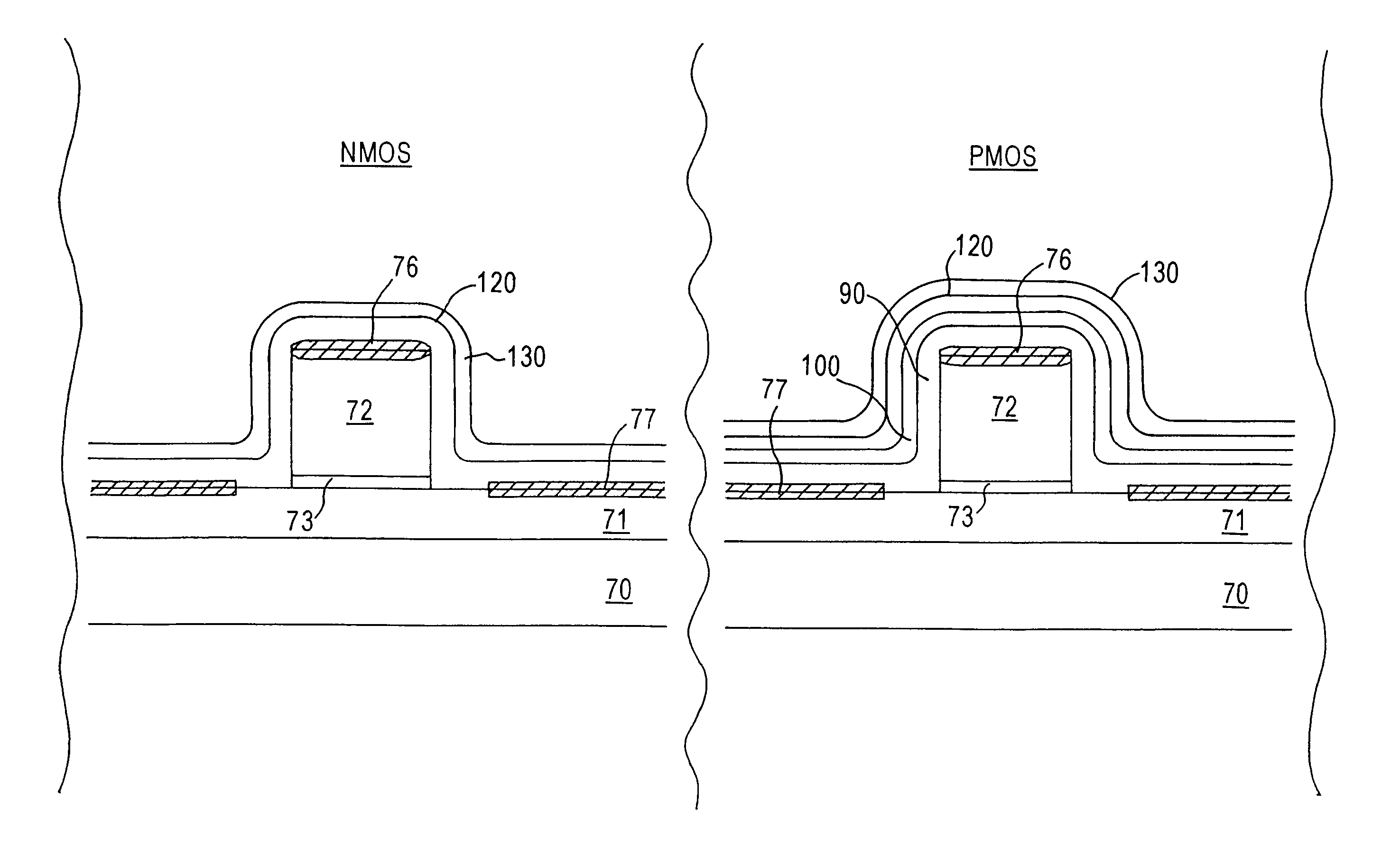
[0021]Transistors built on Si—Ge substrates involve different considerations than those built on bulk silicon substrates. Because of the large thickness of silicon substrates, stressed films deposited thereon tend to affect the substrate with a stress opposite to that exhibited by the film. For example, if a tensile stressed film is deposited on a bulk silicon substrate, compressive stress is imparted to the substrate and, hence, a channel region. However, typically, and in accordance with embodiments of the present invention, Si—Ge substrates are formed with a strained silicon layer having a thickness of about 200 Å to about 300Å. Relaxed source / drain regions may be formed thereon at a thickness of up to about 400 Å. Thus, the thickness of the strained Si layer and drain / source regions together typically does not exceed 800 Å. As a result, the strained Si layer, even together with a relaxed Si layer, is relatively transparent to the type of stress exhibited by a film deposited ther...


PUM


Abstract

The carrier mobility in transistor channel regions of Si—Ge devices is increased by employing a stressed liner. Embodiments include applying a high compressive or tensile stressed film overlying relaxed source / drain regions. Other embodiments include applying a high compressively or high tensilely stressed film, after post silicide spacer removal, over gate electrodes and strained Si source / drain regions of P-channel or N-channel transistors, respectively.

Description

FIELD OF THE INVENTION[0001]The present invention relates to micro-miniaturized semiconductor devices comprising transistors on silicon-germanium. The present invention is particularly applicable in fabricating transistors with enhanced channel carrier mobility.BACKGROUND OF THE INVENTION[0002]The relentless pursuit of miniaturized high speed semiconductor devices continues to challenge the limitations of conventional semiconductor materials and fabrication techniques. Conventional semiconductor devices typically comprise a plurality of active devices in or on a common semiconductor substrate, e.g., CMOS devices comprising at least a pair of PMOS and NMOS transistors in spaced adjacency. Current technology utilizes crystalline semiconductor wafers as substrates, such as a lightly p-doped epitaxial (“epi”) layer of silicon (Si) grown on a heavily-doped, crystalline Si Substrate. The low resistance of the heavily-doped substrate is necessary for minimizing susceptibility to latch-up, ...

Claims


Application Information

Patent Timeline
Patent Type & Authority Patents(United States)
IPC IPC(8): H01L31/072H01L21/336H01L21/8238H01L29/10
CPCH01L21/823807H01L21/823828H01L29/1054H01L29/7843H01L29/6653H01L29/6656H01L29/665
Inventor SUN, SEY-PINGBROWN, DAVID E.
Owner ADVANCED MICRO DEVICES INC
Why Eureka
Try Eureka