Method of precise laser nanomachining with UV ultrafast laser pulses

a laser nano-machining and ultra-fast technology, applied in nanoinformatics, manufacturing tools, instruments, etc., can solve the problems of high-cost techniques usually requiring stringent environmental conditions, difficult to meet size and positioning accuracy requirements of conventional laser micro-machining methods, and complicated manufacturing of materials

Inactive Publication Date: 2006-06-06
PANASONIC CORP
View PDF3 Cites 89 Cited by
  • Summary
  • Abstract
  • Description
  • Claims
  • Application Information

AI Technical Summary

Problems solved by technology

The feature sizes used to form photonic crystals and the precise alignment requirements of these features complicate manufacture of these materials.
Traditionally, both these feature size and positioning accuracy requirements have been difficult to meet with conventional laser micromachining methods.
These high-cost techniques usually require stringent environmental conditions, such as high vacuum or clean room condition.
Thus, in system where a visible or an IR laser is used for nanomachining, the spot size is undesirably large for forming submicron features, even if high numerical aperture (low f#) optics are used.
However, this technique has a number of drawbacks for precise nanomachining, since the center of area actually machined may be somewhat offset from the center of the intensity profile.
This uncertainty of the machining center may be induced by defects or imperfections of the material being processed, or may be due to slight pulse-to-pulse variations in the beam profile.
Additionally, as the ratio of the machined area to the beam spot decrease, reducing any fluence fluctuations between pulses becomes increasingly critical.
Because most of these lasers have a pulse duration of >1 ns, they may cause undesirable heat effected zones to develop in the surrounding material during machining.
Thus, these lasers may be undesirable for many nanomachining applications.

Method used


Image

  • Method of precise laser nanomachining with UV ultrafast laser pulses
  • Method of precise laser nanomachining with UV ultrafast laser pulses
  • Method of precise laser nanomachining with UV ultrafast laser pulses

Examples


Embodiment Construction

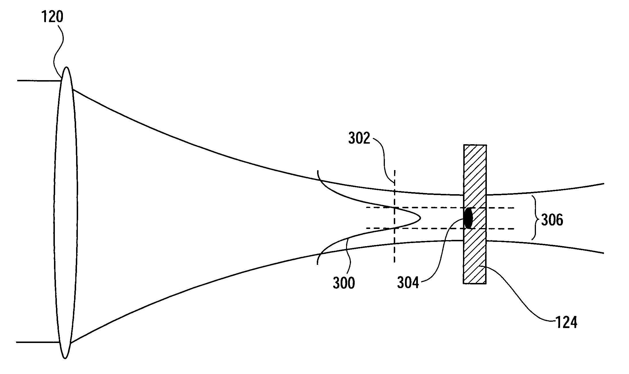
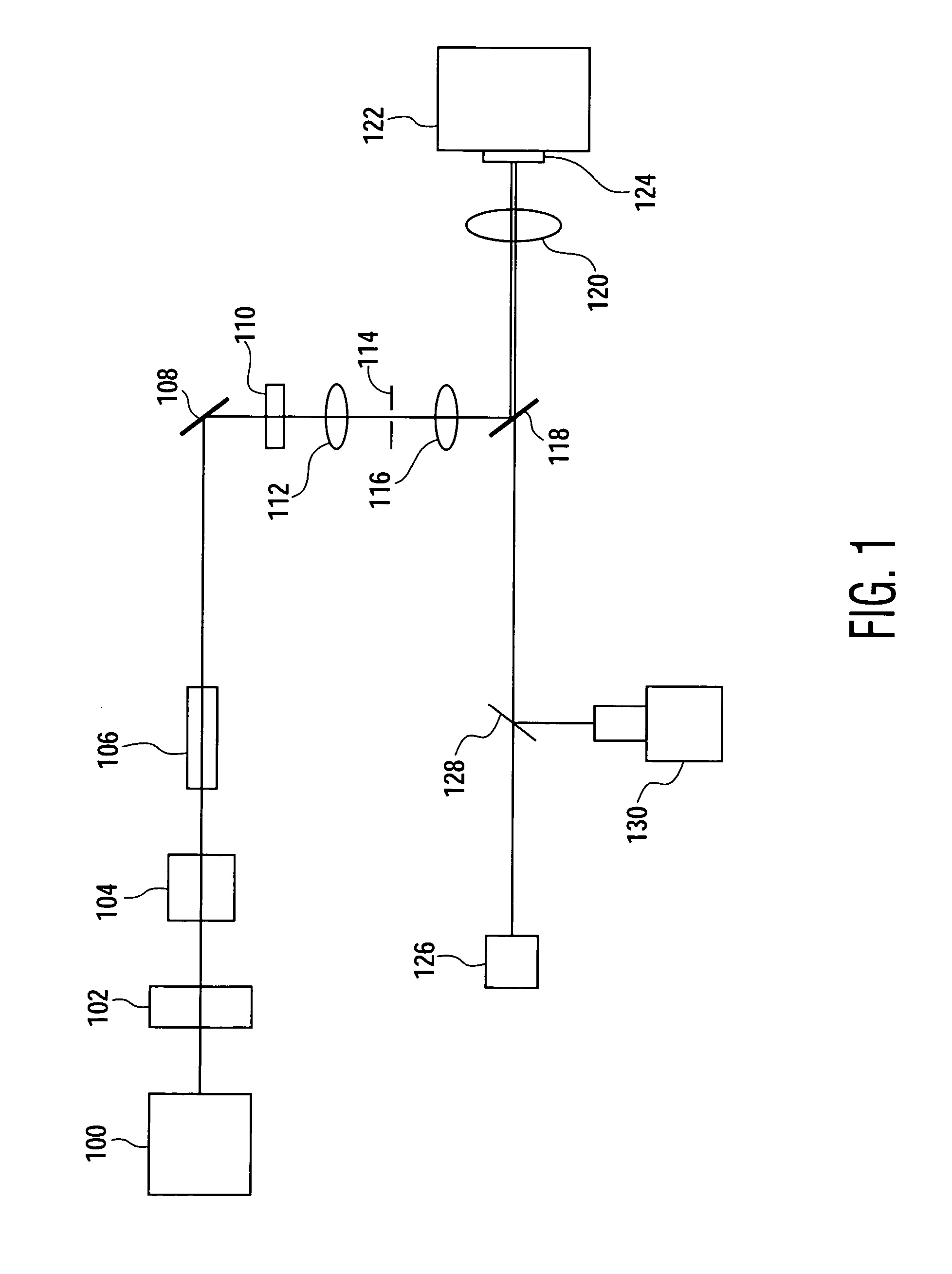
[0023]FIG. 1 illustrates a simplified block diagram of an exemplary laser micro-machining system according to the present invention. This exemplary system includes: ultrafast laser oscillator 100; shutter 102; variable attenuator 104; harmonic generating crystal 106; dichroic mirrors 108 and 118; polarization control means 110; lenses 112, 116, and 120; mask 114; work piece holder 122; work piece illumination source 126; beam splitter 128; and digital camera 130. The optical beams in the exemplary system are shown as dotted lines.

[0024]In this exemplary system, ultrafast laser oscillator 100 may desirably include any type of solid state gain medium typically used for ultrafast laser machining applications, such as: Cr:YAG (peak fundamental wavelength, λf=1520 nm); Cr:Forsterite (λf=1230–1270 nm); Nd:YAG and Nd:YVO4 (λf=1064 nm); Nd:GdVO4 (λf=1063 nm); Nd:YLF (λf=1047 nm and 1053 nm); Nd:glass (λf=1047–1087 nm); Yb:YAG (λf=1030 nm); Cr:LiSAF (λf=826–876 nm); Ti:Sapphire (λf=760–820 n...


PUM

PropertyMeasurementUnit
peak wavelengthaaaaaaaaaa
diameteraaaaaaaaaa
FWHMaaaaaaaaaa

Abstract

A method for manufacturing a microstructure, which includes at least one feature having a dimension less than 200 nm, on a work piece. Pulses of UV laser light having a duration of less than about 1 ps and a peak wavelength of less than about 380 nm are generated. These pulses of UV laser light are focused to a substantially diffraction limited beam spot within a target area of the work piece. The fluence of this substantially diffraction limited beam spot in the target area of the work piece is controlled such that the diameter of the section of the target area machined by one of the pulses of UV laser light is less than 200 nm.

Description

FIELD OF THE INVENTION[0001]The present invention concerns a method for micro- and nano-machining of features smaller than 200 nm on microstructures using UV ultrafast laser pulses. This method may also allow the laser machining of features smaller than 200 nm.BACKGROUND OF THE INVENTION[0002]As products get smaller and smaller, there is greater demand for micro-electrical-mechanical systems (MEMS), micro-optical devices and photonic crystals. With this demand, there is an associated increased interest in micro- and nano-machining. There are numerous possible applications for MEMS. As a breakthrough technology, allowing unparalleled synergy between previously unrelated fields such as biology and microelectronics, many new MEMS applications have emerged and many more may emerge in the near future, expanding beyond those currently identified or known. Additional applications in quantum electric devices, micro-optical devices and photonic crystals are also emerging.[0003]Here are a few...

Claims


Application Information

Patent Timeline
Patent Type & Authority Patents(United States)
IPC IPC(8): B23K26/02B23K26/04B23K26/073B81C99/00G01Q40/00G01Q60/00
CPCB23K26/04B23K26/073B23K26/043B82Y30/00B82Y10/00
Inventor LI, MING
Owner PANASONIC CORP
Why Eureka
Try Eureka