Integrated type probe card and its fabrication method

a probe card and integrated technology, applied in the field of probe cards, can solve the problems of affecting test stability, requiring a lot of fabrication time, and requiring a lot of labor to install probes, and achieve the effects of reducing manufacturing costs, eliminating noise, and convenient adjustmen

Inactive Publication Date: 2006-06-06
IND TECH RES INST
View PDF9 Cites 10 Cited by
  • Summary
  • Abstract
  • Description
  • Claims
  • Application Information

AI Technical Summary

Benefits of technology

[0007]The present invention has been accomplished under the circumstances in view. It is one object of the present invention to provide an integrated type probe card, which has the probes integrated, reducing the manufacturing cost. It is another object of the present invention to provide an integrated type probe card, which enables the level status of the probes to be conveniently adjustable. It is still another object of the present invention to provide an integrated type probe card, which eliminates the production of noises during signal transmission.
[0008]To achieve these and other objects of the present invention, the integrated type probe card comprises a plurality of probes; a circuit space converter, the circuit space converter comprising multiple layers of circuits therein, and a plurality of first contacts and second contacts respectively arranged at two opposite sides of the multiple layers of circuits and electrically connected to the circuits, the density of the first contacts being higher than the second contacts, the first contacts being respectively connected to the probes for transmitting signal from the probes to the second contacts; a spring connector plate, the spring connector plate comprising a holder plate, the holder plate having a predetermined number of receiving holes extended through top and bottom sides thereof, and a plurality of metal spring members respectively mounted in the receiving holes of the holder plate, the metal spring members each having two distal ends respectively protruded over the top and bottom sides of the holder plate and having one of the respective two distal ends respectively electrically connected to the second contacts of the circuit space converter; a circuit board pressed on one of the two distal ends of each of the metal spring members against the second contacts of the circuit space converter, the circuit board having a plurality of circuits and contacts arranged on one side thereof and electrically connected to the metal spring members of the spring connector plate for testing electric signal transmitted from the probes; and a level adjustment mechanism adapted to hold the probes, the circuit space converter, the spring connector plate and the circuit board in order and to adjust the level status of the circuit space converter, for enabling the metal spring members to compensate elevational difference between the circuit space converter and the spring connector plate and to keep the circuit space converter electrically connected to the circuit board.

Problems solved by technology

These probe cards or electrical contactor assemblies are different in structural design, principle of action and method of fabrication, however they commonly have numerous drawbacks.
These two types require much labor to install probes (tungsten contact pins, lead contact pins, or steel contact pins) in the circuit board individually and to adjust the heights of the probes.
Because of much human labor is used during fabrication, much fabrication time is required and unequal level status of the probes may affect test stability.
Because each probe has a big part exposed to the outside without insulation, parasitic capacitance and induction may produce, resulting in attenuation of high frequency test signal and increase of crosstalk.
If the surface of the circuit board under test is not in level, low deformability of probes cannot keep all probes in effective contact with the test points.
Further, there is a limitation to probe installation density by labor.
High pin counts results in high manufacturing cost.
This pin count limitation imparts a barrier to the development of electronic elements.
The gap between each two adjacent spring members is insufficient to eliminate crosstalk, and signal error may be produced.
Crosstalk may cause an inaccurate test result.

Method used


Image

  • Integrated type probe card and its fabrication method
  • Integrated type probe card and its fabrication method
  • Integrated type probe card and its fabrication method

Examples


Embodiment Construction

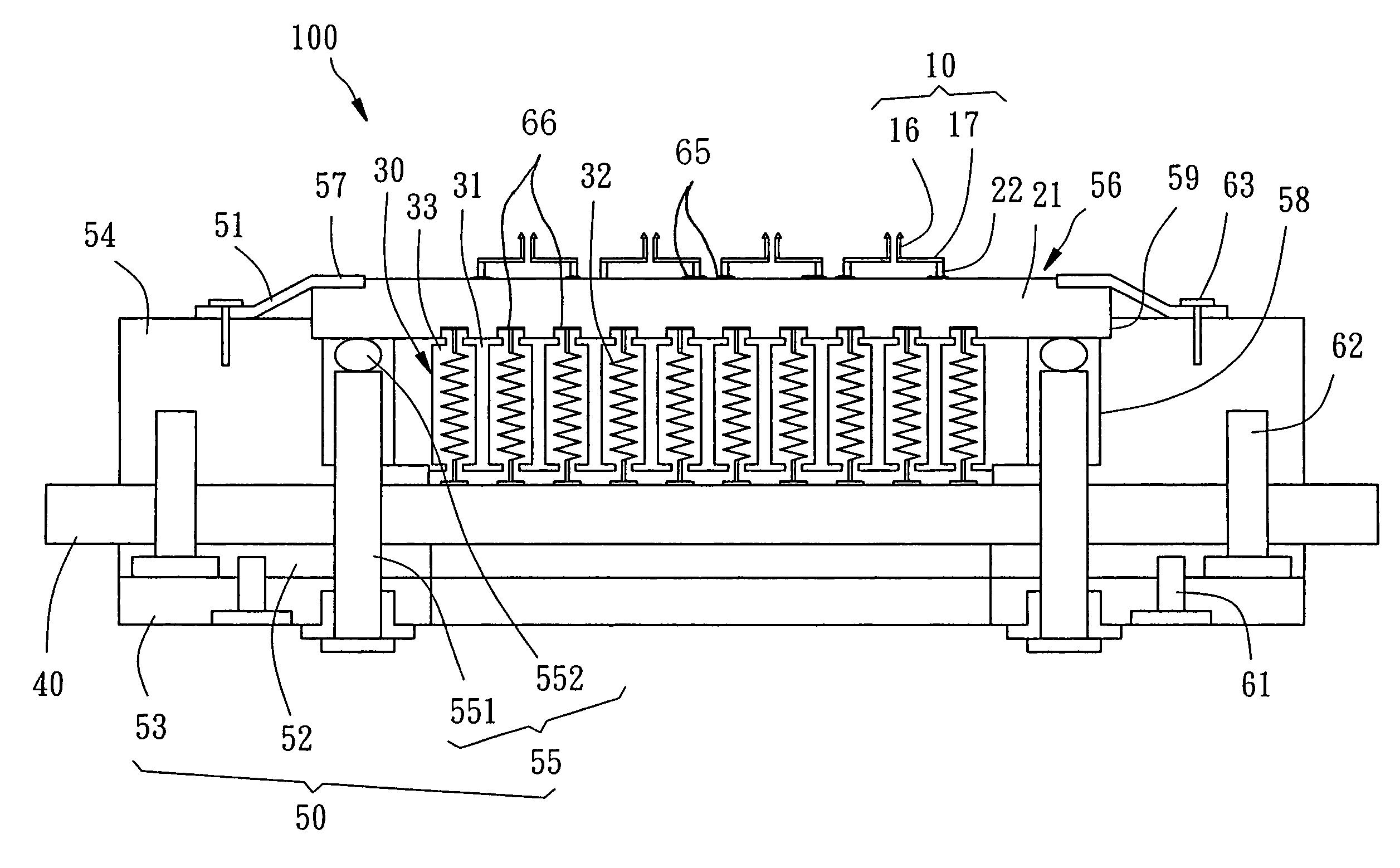
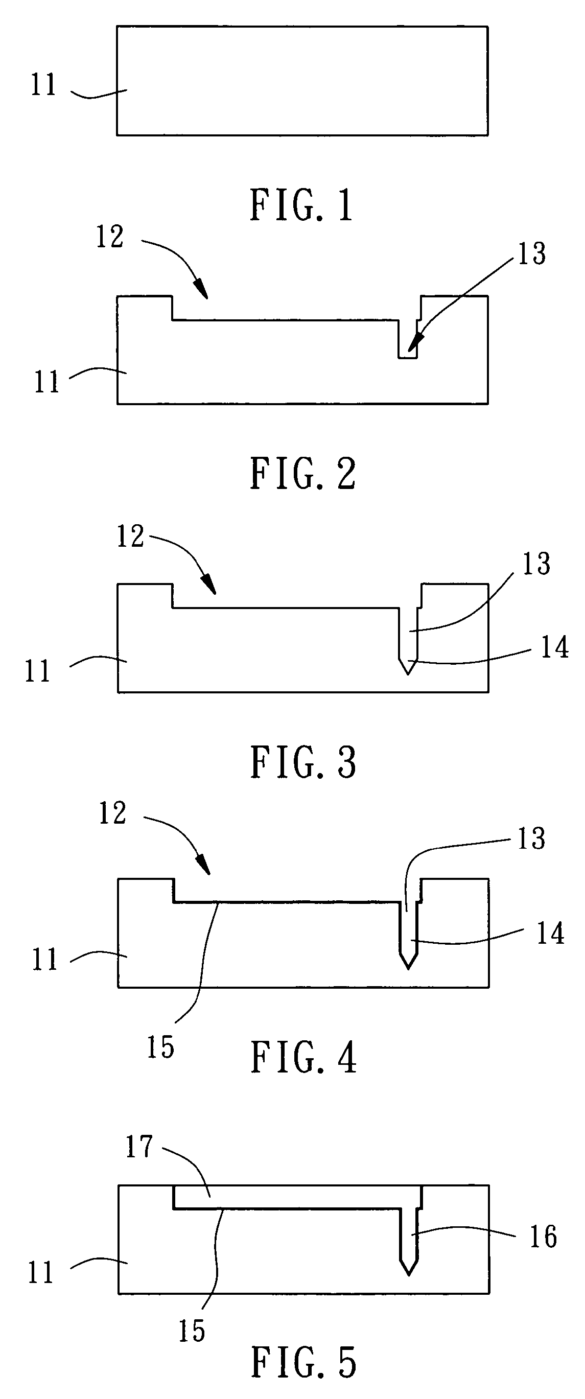
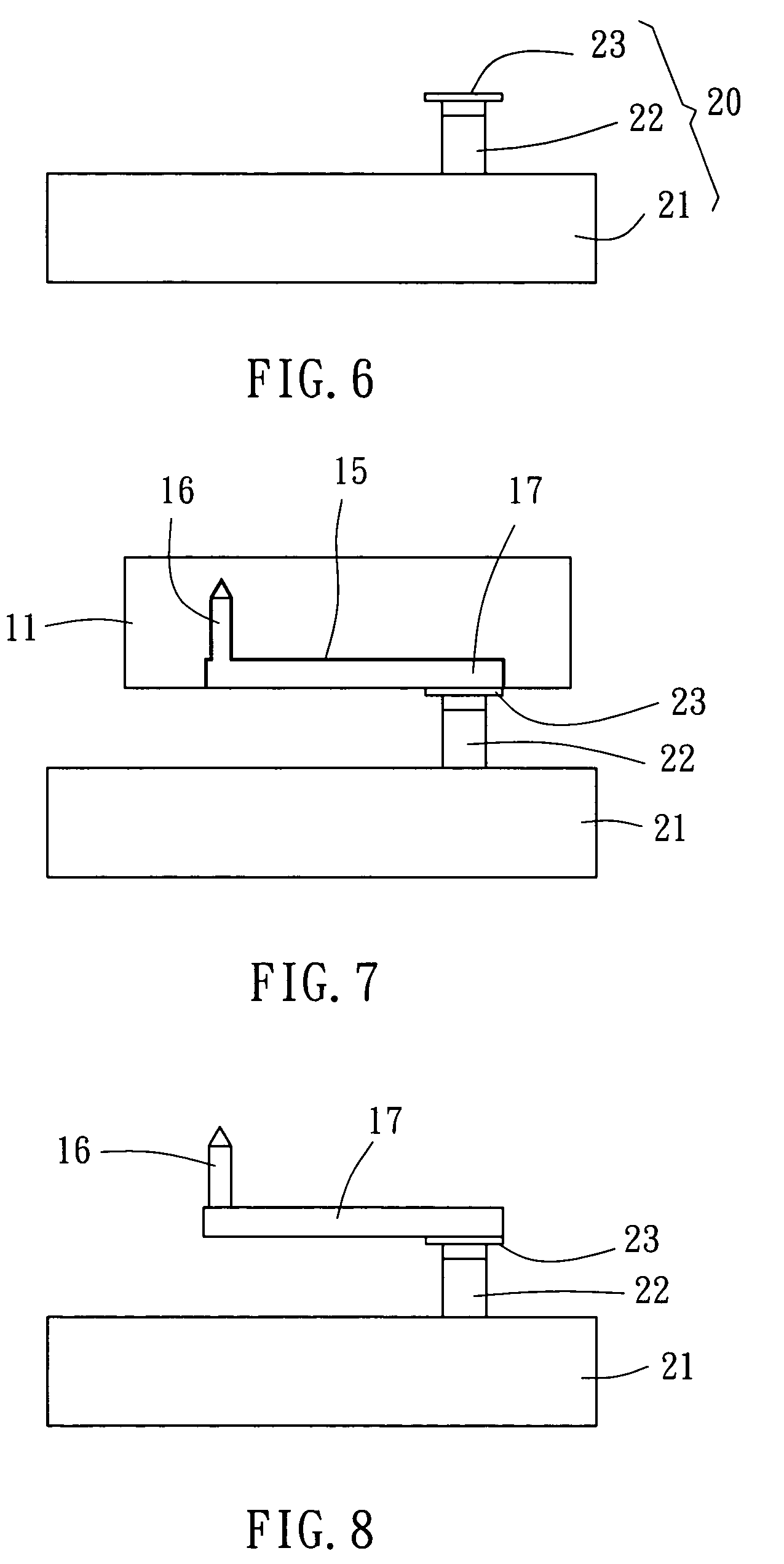
[0020]Referring to FIGS. 1˜11, an integrated type probe card 100 is shown comprised of a predetermined number of probes or contacts 10, a circuit space converter 20, a spring connector plate 30, a circuit board 40, and a level adjustment mechanism 50.

[0021]The probes 10 are made subject to the following Steps I˜IV:

[0022]Step I: Material preparation. As shown in FIG. 1, a strip-like substrate, for example, a silicon wafer 11 is prepared and pre-treated with washing, drying, and other requisite pre-treatment processes (FIG. 1 is a side view in section of the silicon wafer).

[0023]Step II: Substrate etching. As shown in FIG. 2, LIGA (Lithography process) is employed to precisely define the geometrical shape and locations of probe tips, and then anisotropic etching is employed to etch the silicon wafer 11 to a predetermined depth by means of RIE (Reactive Ion Etching) so as to form elongated cantilever spaces 12 of high aspect ratio, and then anisotropic etching is repeated to etch one e...


PUM


Abstract

An integrated type probe card includes a circuit space converter having first and second contacts arranged at different density at two sides, probes connected to the contacts at one side of the circuit space converter that are arranged at a high density probes; a spring connector plate, which holds metal spring members in respective receiving holes thereof, a circuit board pressed on the metal spring members against the contacts at the other side of the circuit space converter that are arranged at a low density, and a level adjustment mechanism that accommodates the probes, the circuit space converter, the spring connector plate and the circuit board and enables the user to adjust the level status of the circuit space converter, keeping the circuit space converter electrically connected to the circuit board for transmitting test signal from the probes to the circuit board.

Description

BACKGROUND OF THE INVENTION[0001]1. Field of the Invention[0002]The present invention relates to a probe card or electrical contactor assembly and more particularly, to an integrated type probe card. The invention relates also to the fabrication of the integrated type probe card.[0003]2. Description of the Related Art[0004]Various probe cards or electrical contactor assemblies are seen in U.S. Pat. Nos. 4027935; 4754256; 5090118; 5475318; 6072190. These probe cards or electrical contactor assemblies are different in structural design, principle of action and method of fabrication, however they commonly have numerous drawbacks. Regular probe cards include cantilever type, for example, epoxy ring probe cards, and vertical type, for example, cobra probe cards. These two types require much labor to install probes (tungsten contact pins, lead contact pins, or steel contact pins) in the circuit board individually and to adjust the heights of the probes. Because of much human labor is used...

Claims


Application Information

Patent Timeline
Patent Type & Authority Patents(United States)
IPC IPC(8): G01R31/26G01R31/28
CPCG01R31/2889
Inventor CHANG, JYH-CHUNWANG, HORNG-JEECHOU, MIN-CHIEHPAN, KUN-CHIHHUANG, YA-JUTSAI, CHU-SHUCHEN, CHIH-WEI
Owner IND TECH RES INST
Why Eureka
Try Eureka