Hybrid orientation substrates by in-place bonding and amorphization/templated recrystallization

a hybrid orientation substrate and in-place bonding technology, applied in semiconductor/solid-state device manufacturing, basic electric elements, electric devices, etc., can solve the problems of damage layer interfering with the clean recrystallization of the amorphized region, damaged crystalline layer between the amorphized, damaged crystalline layer, etc., to achieve densification and free amorphized regions

Inactive Publication Date: 2006-06-13
IBM CORP
View PDF5 Cites 93 Cited by
  • Summary
  • Abstract
  • Description
  • Claims
  • Application Information

AI Technical Summary

Benefits of technology

[0027]With the first embodiment of top amorphization and bottom templating, amorphization can proceed without EOR damage to the substrate semiconductor layer because the EOR damage is absorbed by the sacrificial spacer layer. With the second embodiment of top templating and bottom amorphization, amorphization will leave beginning-of-range defects primarily in the sacrificial spacer layer. In both cases, the in-place bonding will leave a sharp interface between the amorphized semiconductor and the templating crystalline semiconductor, and the templating semiconductor will largely be free of defects. If desired, some annealing may be performed prior to in-place bonding to heal beginning-of-range defects in the upper semiconductor layer, and / or to slightly densify the amorphized regions. While the conditions for this pre-crystallization annealing must be mild enough to avoid spontaneous crystallization of the amorphized regions, there is no problem with annealing at the lower (but still elevated) temperatures at which templated recrystallization would occur, since amorphized and templating layers are not yet in direct contact.

Problems solved by technology

A potential problem with this way of implementing ATR is that the ion implant methods typically used for amorphization leave a damaged crystalline layer between the amorphized and the non-amorphized regions of the bilayer template stack.
This EOR damage layer interferes with the clean recrystallization of the amorphized region, both by introducing threading defects (that can propagate to the wafer's surface) and by leaving a band of dislocation loops at the position of the original damage layer.
However EOR damage (or “beginning-of-range” damage for the case of top templating and bottom amorphization, when ion implantation is used to form a buried amorphous layer) is a characteristic of all ion implantation processes and is very difficult to avoid.
An additional difficulty with previous ATR methods of forming hybrid orientation substrates is that they require direct semiconductor-to-semiconductor (typically Si-to-Si) bonding.
This is normally achieved with hydrophobic bonding, a bonding technique that is more difficult and less well developed than the more commonly used hydrophilic bonding.
In addition, the widely used surface plasma treatments developed to allow room temperature bonding typically introduce surface oxygen, making them incompatible with an oxide-free bonded interface.
Bonding at higher temperatures also can present difficulties, since most cleaving processes (used to separate the bonded layer from the wafer to which it was originally attached) are thermally activated and start occurring in the same temperature range as the bonding.
However, hybrid orientation substrates formed by this technique have the drawback that they are inherently non-planar (since the semiconductor island 330′ is higher than the exposed regions of semiconductor 310 adjacent to the island).

Method used


Image

  • Hybrid orientation substrates by in-place bonding and amorphization/templated recrystallization
  • Hybrid orientation substrates by in-place bonding and amorphization/templated recrystallization
  • Hybrid orientation substrates by in-place bonding and amorphization/templated recrystallization

Examples


Embodiment Construction

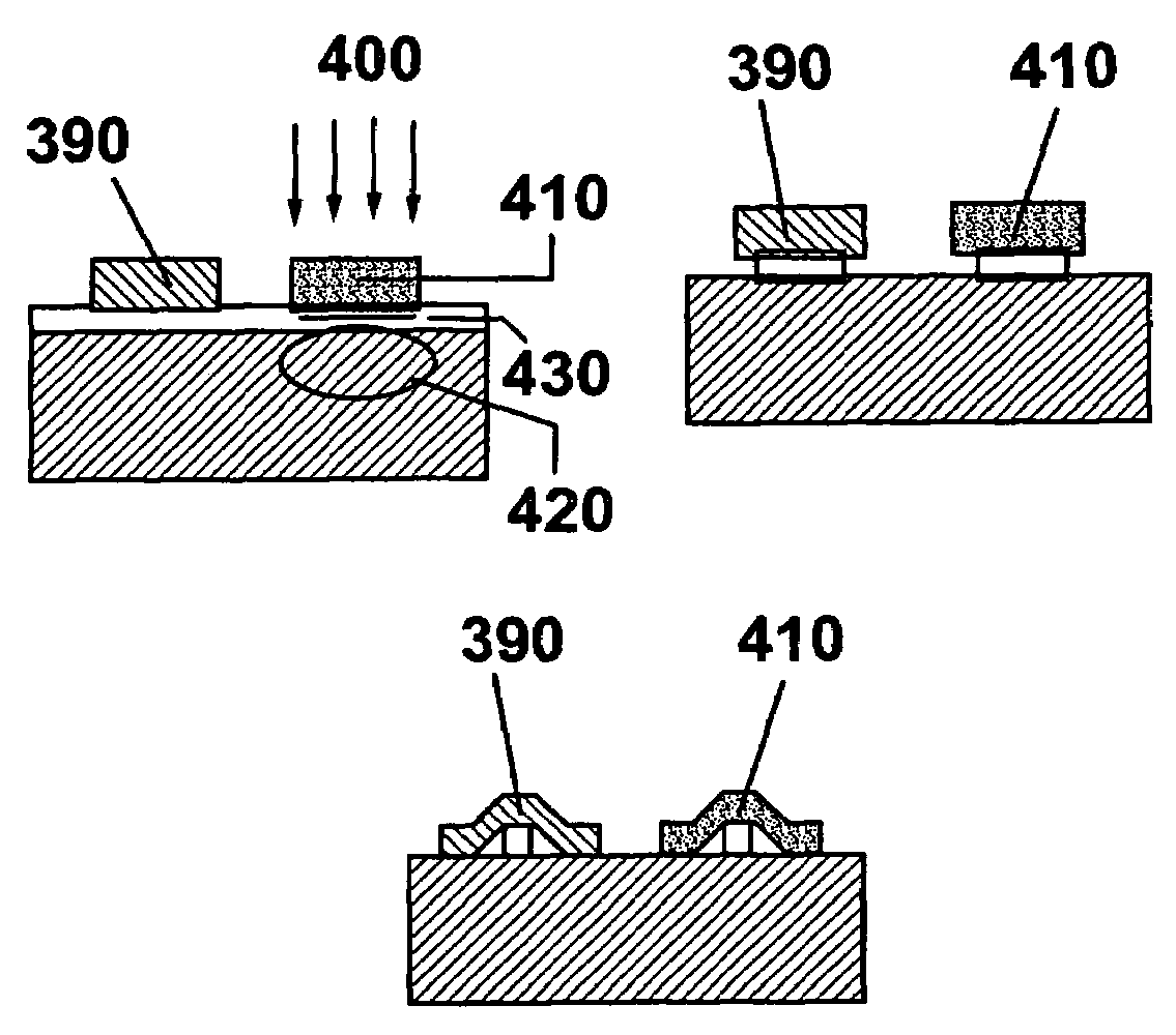
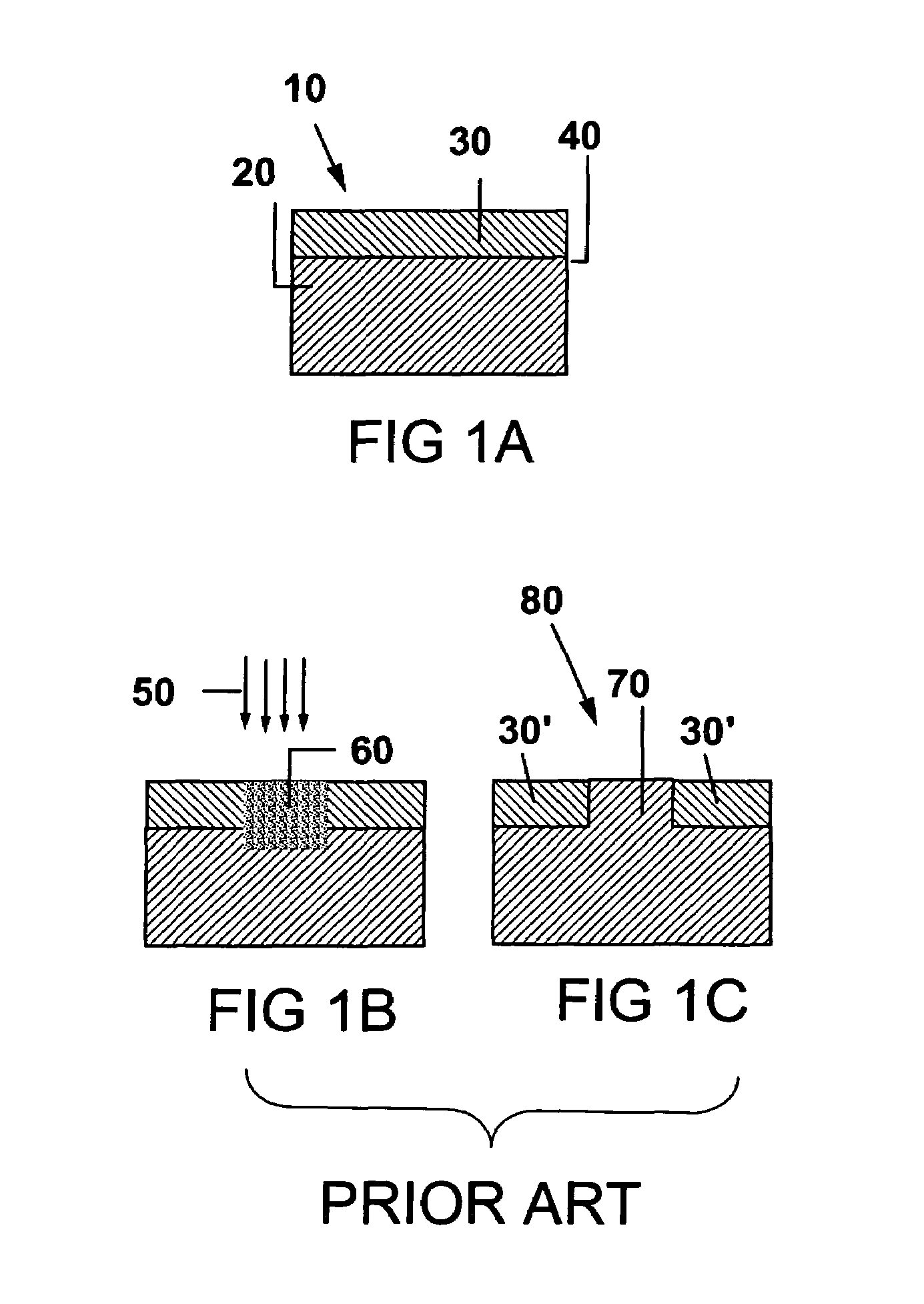
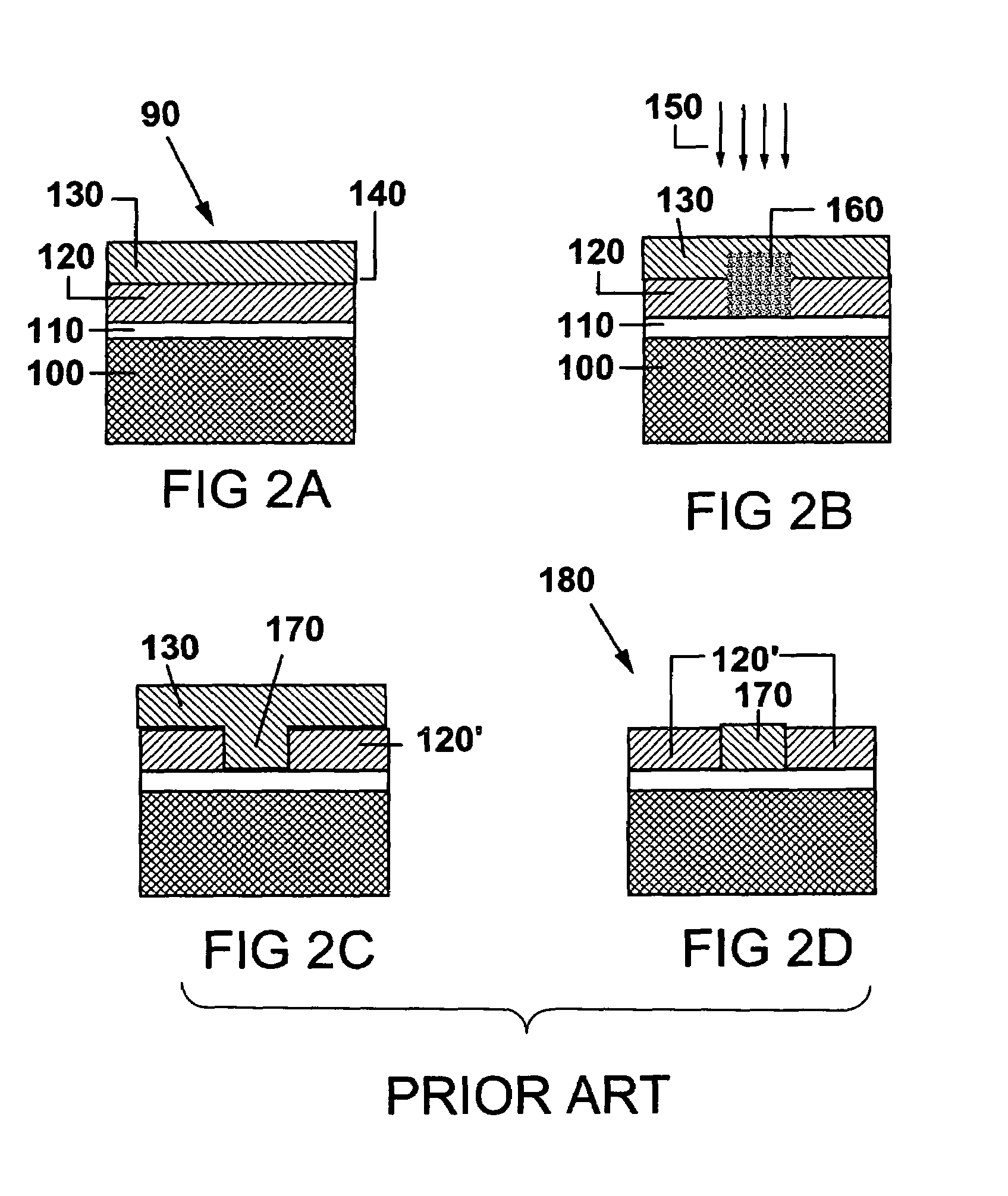
[0046]The present invention, which provides methods of fabricating planar hybrid-orientation substrate structures, will now be described in greater detail by referring to the drawings that accompany the present application. The drawings that accompany the present application are provided for illustrative proposes and thus they are not drawn to scale. In the drawings, which illustrate the process flows of the present invention, reference numbers are not shown for materials (or areas) that are not be affected by the specified processing step. It is understood then that the materials not labeled in a particular step have not changed from the proceeding step(s). Also, in the drawings, like and / or corresponding materials are described with like reference numerals.

[0047]As mentioned above, the methods of the present invention share the following basic steps of: selecting a starting substrate comprising a first single crystal semiconductor layer having a first crystal orientation overlying...


PUM


Abstract

A method utilizing in-place bonding and amorphization/templated recrystallization (ATR) is provided for making bulk and semiconductor-on-insulator substrates having coplanar semiconductor layers of different crystallographic orientations. First and second semiconductor layers having different orientations are bonded to opposite sides of a sacrificial spacer layer. Selected areas in one of the semiconductor layers are amorphized; in-place bonding is then performed in a wet etch solution to remove the sacrificial layer and leave the semiconductor layers bonded to each other. The amorphized regions are recrystallized across the bonded interface, using the semiconductor on the non-amorphized side of the bonded interface as a template.

Description

RELATED APPLICATIONS[0001]This application is related to pending U.S. application Ser. No. 10 / 725,850, filed Dec. 2, 2003, entitled “Planar substrate with selected semiconductor crystal orientations formed by localized amorphization and recrystallization of stacked template layers,” the content of which is incorporated by reference. Likewise, this application is related to U.S. application Ser. No. 10 / 978,551, filed Nov. 1, 2004, entitled “In-place bonding of microstructures,” the content of which is also incorporated herein by reference.FIELD OF THE INVENTION[0002]The present invention relates to high-performance complementary metal oxide semiconductor (CMOS) circuits in which carrier mobility is enhanced by utilizing different semiconductor surface orientations for p-type field effect transistors (FETs) and n-type FETs. More particularly, the present invention relates to methods for fabricating planar substrate structures with different surface crystal orientations, and to the hyb...

Claims


Application Information

Patent Timeline
Patent Type & Authority Patents(United States)
IPC IPC(8): H01L21/762
CPCH01L21/823807H01L21/84H01L21/823878H01L21/02002
Inventor COHEN, GUY MOSHESAENGER, KATHERINE L.
Owner IBM CORP
Why Eureka
Try Eureka