Memory device and method of manufacturing including deuterated oxynitride charge trapping structure

a technology of deuterated oxynitride and memory device, which is applied in the direction of semiconductor devices, basic electric elements, electrical apparatus, etc., can solve the problems of significant source of charge retention problems, poor charge retention, and low threshold cell charge loss, so as to reduce the number of available dangling bonding sites and improve data retention characteristics. , the effect of reducing the number of hydrogen inclusions in the structur

Active Publication Date: 2006-06-13
MACRONIX INT CO LTD +1
View PDF15 Cites 48 Cited by
  • Summary
  • Abstract
  • Description
  • Claims
  • Application Information

AI Technical Summary

Benefits of technology

[0010]The present invention provides a method for manufacturing a charge storage stack with improved data retention characteristics, applicable for use in very small memory devices. The method includes the formation of a stack including a bottom dielectric layer, a charge trapping structure on the bottom dielectric layer, and a top dielectric layer. The bottom dielectric layer, the charge trapping structure, and the top dielectric layer each comprise silicon oxynitride, and are formed using reactant gases that comprise hydrogen, where the hydrogen comprises at least 90 percent deuterium isotope. The bottom dielectric layer, charge trapping structure, and top dielectric layer include hydrogen inclusions which can be described for the purposes of description as being attached to dangling silicon bonding sites that result from manufacturing processes that include reaction gases comprising hydrogen. The bottom dielectric layer, charge trapping structure, and top dielectric layer each have respective relative concentrations of oxygen and nitrogen. The relative concentrations of nitrogen in the charge trapping structure is high enough for the material to act as a charge trapping structure with an energy gap that is lower than the energy gaps in the bottom dielectric layer and the top dielectric layer. The presence of oxygen in the charge trapping structure reduces the number of available dangling bonding sites, and thereby reduces the number of hydrogen inclusions in the structure. A combination of utilizing deuterium isotope in the reactant gases and silicon oxynitride as the charge trapping structure, substantially reduces the number of hydrogen inclusions, and of those inclusions, reduces the number which are not deuterium isotope.
[0011]The top and bottom dielectrics are formed in embodiments of the described process using radical oxidation processes that include in situ radical formation, such as in situ steam generation ISSG, resulting in high-quality ultrathin layers of oxide, including bottom dielectric layers less than 7 nanometers thick in some embodiments, and less than 3 nanometers thick in other embodiments. The layers of oxide can be treated with, or formed in the presence of, a nitrogen containing material. The nitrogen containing material comprises hydrogen in some embodiments, in which the hydrogen comprises at least 90 percent deuterium isotope. Use of nitrogen containing oxides in the bottom and top dielectric layers provides improved resistance to breakdown, including resistance to boron penetration which degrades device durability. The use of in situ radical oxidation processes, combined with deuterated reactant gas and nitrogen treatments in the top and bottom dielectric further enhances performance of the charge storage stack.
[0012]The technology described herein provides a new memory device with improved durability and charged retention characteristics. A memory device comprises the terminal, such as a source or drain having a first conductivity type in a substrate, the region in the substrate adjacent the terminal having a second conductivity type, the bottom dielectric over portions of the terminal in the region, the charged storage structure on the bottom dielectric, and the top dielectric over the charged storage structure. As mentioned above, the bottom dielectric layer, the charge trapping structure, and the top dielectric layer each comprise silicon oxynitride, and are formed using reactant gases that comprise hydrogen, where the hydrogen comprises at least 90 percent deuterium isotope. The bottom dielectric layer, charge trapping structure, and top dielectric layer include hydrogen inclusions which can be described for the purposes of description as being attached to dangling silicon bonding sites that result from manufacturing processes that include reaction gases comprising hydrogen. The bottom dielectric layer, charge trapping structure, and top dielectric layer each have respective relative concentrations of oxygen and nitrogen. The relative concentrations of nitrogen in the charge trapping structure is high enough for the material to act as a charge trapping structure with an energy gap that is lower at the interfaces between the layers in the stack, than the energy gaps at the interfaces in the bottom dielectric layer and in the top dielectric layer.

Problems solved by technology

Although the erase speed is fast using this technique, the charge retention is poor due to the charge leakage through ultra-thin bottom oxide.
However, the hot hole injection causes oxide damage, leading to charge loss in the high threshold cell and charge gain in the low threshold cell.
The shallow level electrons are a significant source of charge retention problems.
However, leakage of trapped charge, from shallower and deeper traps both, occurs in such devices due to defects in the materials which accumulate over long use, or which are inherent in the structures.
One known class of defects in charge trapping structures is hydrogen inclusions in dielectric layers and structures.

Method used


Image

  • Memory device and method of manufacturing including deuterated oxynitride charge trapping structure
  • Memory device and method of manufacturing including deuterated oxynitride charge trapping structure
  • Memory device and method of manufacturing including deuterated oxynitride charge trapping structure

Examples


Embodiment Construction

[0018]A detailed description of embodiments of the present invention is provided with reference to the FIGS. 2, 3 and 4.

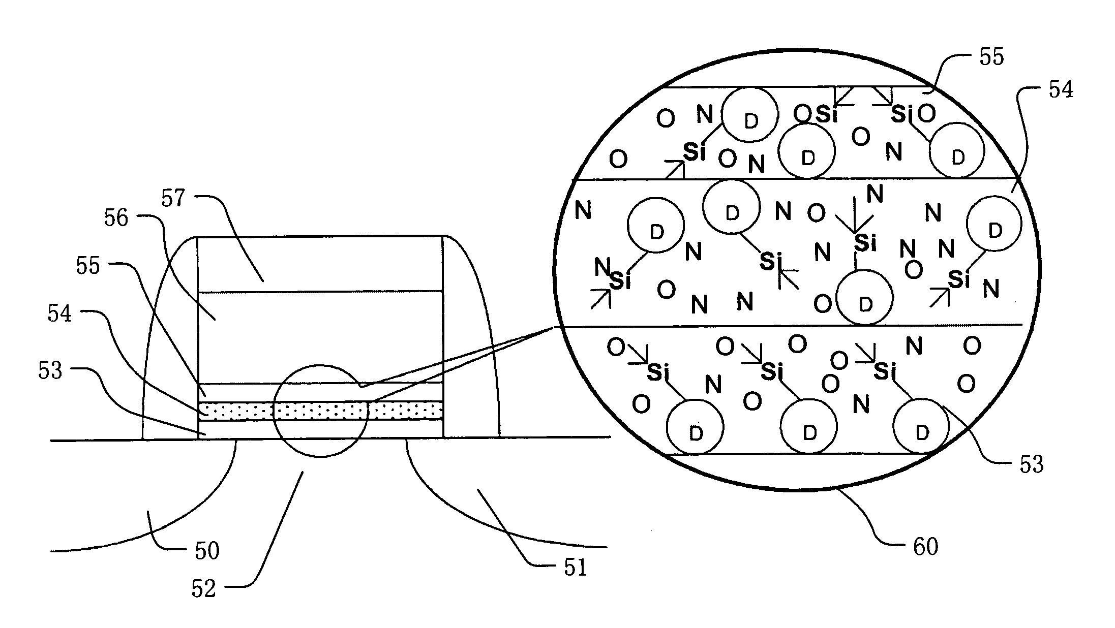
[0019]FIG. 2 provides a graphical representation of a memory cell based on a charge storage stack comprising deuterated oxynitride layers. The memory cell comprises a terminal 50 acting as a source, a terminal 51 acting as a drain and a channel region 52 in the substrate. A bottom dielectric layer 53 overlies the channel region 52 and portions of the source and drain terminals 50, 51. A charge trapping layer 54 overlies the bottom dielectric and a top dielectric 55 overlies the charge trapping layer 54. A gate electrode comprising a polysilicon layer 56 and a silicide layer 57 lie over the top dielectric layer 55. A small region of the bottom dielectric layer 53, charge trapping layer 54 and top dielectric layer are expanded heuristically in the region 60 on the drawing. Silicon atoms are shown schematically with four lines representing the valence electrons normal...


PUM


Abstract

A method for manufacturing a charge storage stack including a bottom dielectric layer, a charge trapping structure on the bottom dielectric layer, and a top dielectric layer, each comprising silicon oxynitride, are formed using reactant gases that comprise hydrogen, where the hydrogen comprises at least 90 percent deuterium isotope. The bottom dielectric layer, charge trapping structure, and top dielectric layer each have respective relative concentrations of oxygen and nitrogen. The relative concentration of nitrogen in the charge trapping structure is high enough for the material to act as a charge trapping structure with an energy gap that is lower than the energy gaps in the bottom dielectric layer and the top dielectric layer. The presence of oxygen in the charge trapping structure reduces the number of available dangling bonding sites, and thereby reduces the number of hydrogen inclusions in the structure.

Description

BACKGROUND OF THE INVENTION[0001]1. Field of the Invention[0002]The present invention relates to nonvolatile memory devices and methods for manufacturing such devices.[0003]2. Description of Related Art[0004]Electrically programmable and erasable nonvolatile memory technologies based on charge storage structures known as EEPROM and flash memory are used in a variety of modern applications. A number of memory cell structures are used for EEPROM and flash memory. As the dimensions of integrated circuits shrink, greater interest is arising for memory cell structures based on charge trapping dielectric layers, because of the scalability and simplicity of the manufacturing processes. Memory cell structures based on charge trapping dielectric layers include structures known by the industry names NROM, SONOS, and PHINES, for example. These memory cell structures store data by trapping charge in a charge trapping dielectric layer, such as silicon nitride. As negative charge is trapped, the ...

Claims


Application Information

Patent Timeline
Patent Type & Authority Patents(United States)
IPC IPC(8): H01L21/322
CPCH01L21/28282H01L29/792Y10S438/954H01L29/40117
Inventor WANG, SZU-YU
Owner MACRONIX INT CO LTD
Why Eureka
Try Eureka