Architecture for an algorithmic analog-to-digital converter

an algorithmic converter and architecture technology, applied in the direction of code conversion, generating/distributing signals, instruments, etc., can solve the problems of low power consumption, slow conversion cycle, and relatively long conversion cycle, and achieve the effect of improving area efficiency and suitably high conversion ra

Active Publication Date: 2006-06-27
SYNAPTICS INC
View PDF23 Cites 34 Cited by
  • Summary
  • Abstract
  • Description
  • Claims
  • Application Information

AI Technical Summary

Benefits of technology

[0005]The present invention provides an algorithmic ADC having an improved area efficiency and a conversion rate suitably high for high speed and bit resolution applications such as video ADC.

Problems solved by technology

Because algorithmic ADCs perform a heavily serial operation using a simple circuit, they are area efficient and consume a low amount of power.
The main disadvantage of algorithmic ADCs is their relatively long conversion cycle occasioned by its serial nature of operation.
For applications such as video analog-to-digital conversion, having resolutions in the range of 7–14 bits and clock frequencies in the range of 20–50 MHz, this conversion cycle is too slow.
Hence, algorithmic topologies have not been suitable for applications such as video ADCs having this speed and resolution range.

Method used


Image

  • Architecture for an algorithmic analog-to-digital converter
  • Architecture for an algorithmic analog-to-digital converter
  • Architecture for an algorithmic analog-to-digital converter

Examples


Embodiment Construction

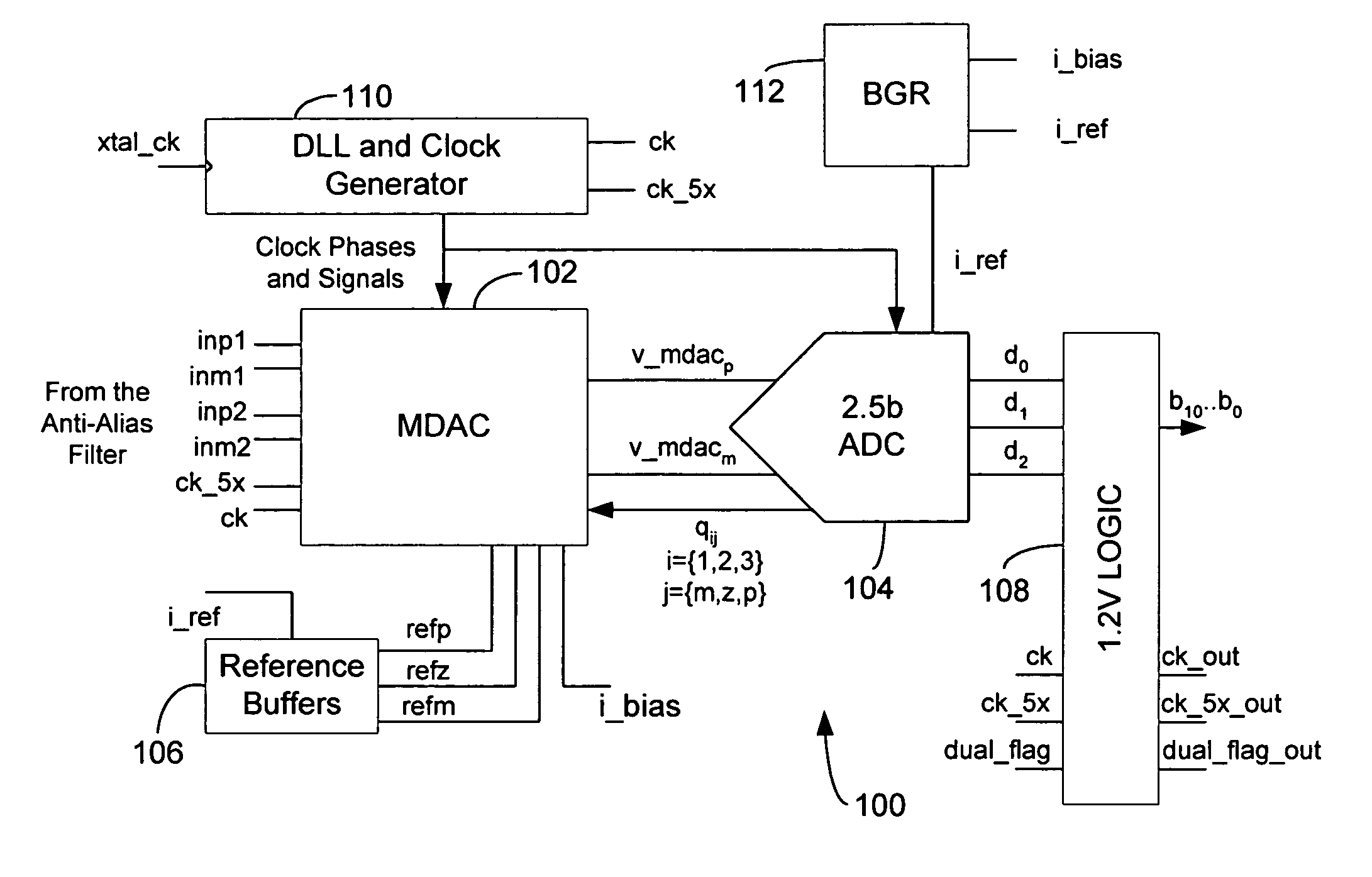
[0036]The present invention provides an algorithmic analog-to-digital converter (ADC) having an improved area efficiency and a conversion rate suitably high for high speed and bit resolution applications such as video ADC. It is area efficient because it contains only one processing unit and has a heavily serial operation principle. By contrast, existing algorithmic ADCs have at least two processing units. The higher conversion rate is achieved by processing multiple bits in each cycle. The processing unit, which employs a switched capacitor topology, resembles a multi-bit stage in a pipelined ADC.

[0037]Overview

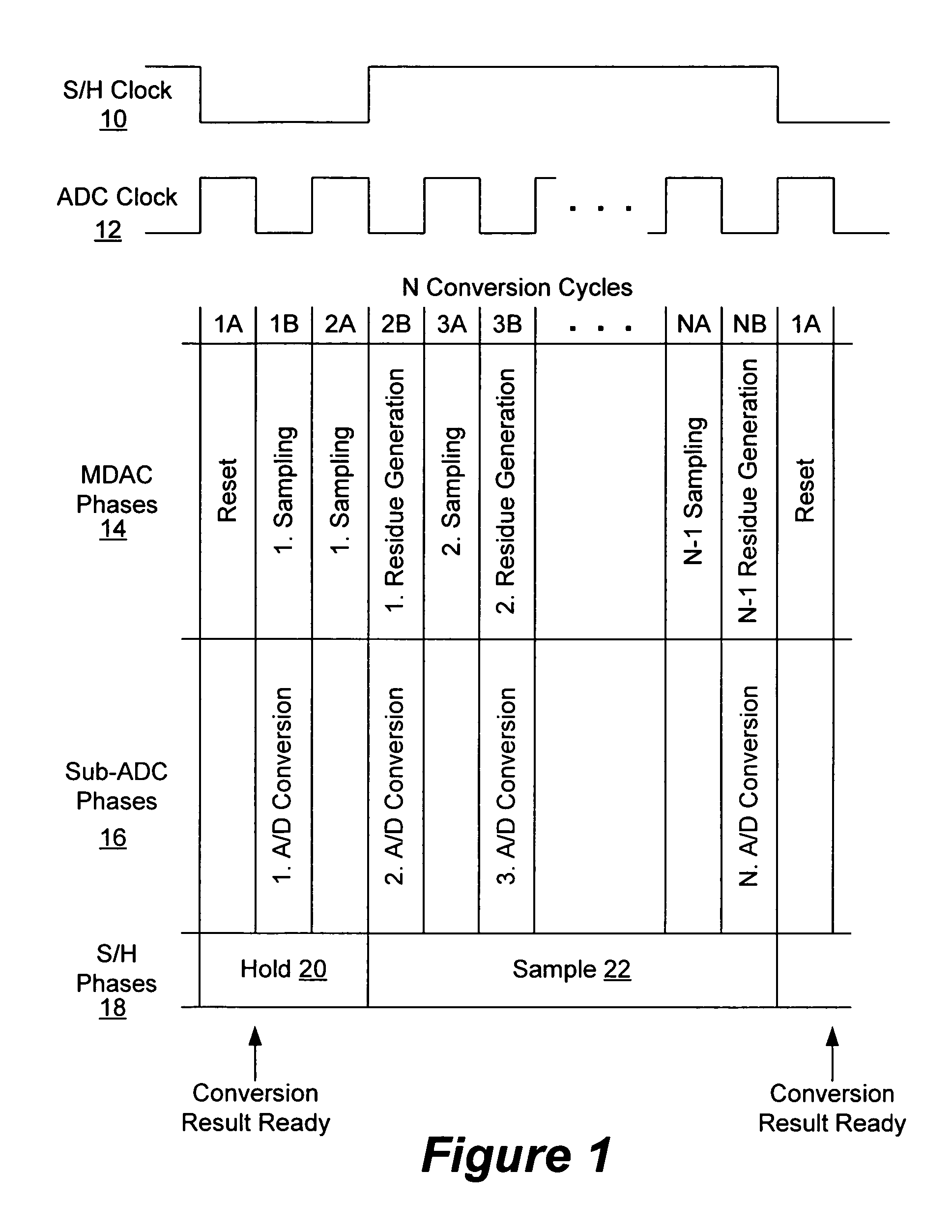
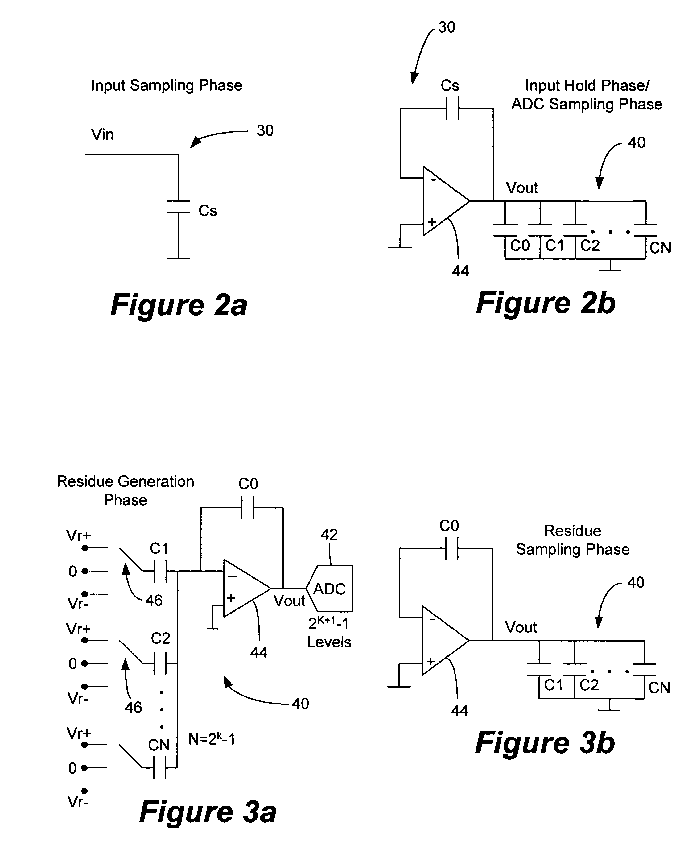
[0038]The architecture comprises a sample-and-hold circuit and a multi-bit serial ADC processing unit (the processing unit, in turn, comprises a multiplying digital-to-analog converter (MDAC) and a sub-ADC). These two circuits work in parallel and share a single operational amplifier. As depicted in FIG. 1, the sample-and-hold circuit works at the sampling rate with uneven du...


PUM


Abstract

An algorithmic analog-to-digital converter (ADC) includes a sample-and-hold circuit and an ADC processing unit operating in parallel and sharing a single operational amplifier. The ADC processing unit includes an MDAC with a switched capacitor topology and a sub-ADC. The ADC processing unit is clocked by an internal clock that is N times faster than the sample-and-hold clock. Each cycle is further sub-divided into two phases. During one phase the capacitors are coupled to a residue or sampled voltage provided by the MDAC, and during another phase the capacitor are coupled to a reference voltage determined by the switch control signals generated by the sub-ADC. A set of data bits is generated by the ADC processing unit during each ADC clock cycle. The N sets of data bits are added to generate the digital output stream.

Description

RELATED APPLICATION[0001]This application is related to the patent application entitled “Clocking Scheme for an Algorithmic Analog-to-Digital Converter” by Mikko Waltari, filed on even date herewith and having common assignee.FIELD OF THE INVENTION[0002]The present invention relates to analog-to-digital converters and, in particular, relates to an area-efficient analog-to-digital converter having an improved algorithmic architecture.BACKGROUND OF THE INVENTION[0003]Analog-to-digital converters (ADCs) are in widespread use. Essentially, the ADC converts a continuous analog signal into discrete bits by sampling the continuous analog signal and quantizing it into a set of discrete levels. There are various types of ADCs, each having different cost and performance characteristics. Algorithmic ADCs (also known as “cyclic” or “recirculating” ADCs) operate by amplifying a signal to be converted and comparing the amplified signal to a reference voltage. If the amplified signal is greater th...

Claims


Application Information

Patent Timeline
Patent Type & Authority Patents(United States)
IPC IPC(8): H03M1/12G06F1/04G06F1/06G06F1/08H03L7/06H03M1/34H03M1/46
CPCH03M1/1245H03M1/466
Inventor WALTARI, MIKKO
Owner SYNAPTICS INC
Why Eureka
Try Eureka