Method of manufacturing electron-emitting device, method of manufacturing electron source, and method of manufacturing image display device

Inactive Publication Date: 2006-07-11
CANON KK
View PDF23 Cites 19 Cited by
  • Summary
  • Abstract
  • Description
  • Claims
  • Application Information

AI Technical Summary

Benefits of technology

[0011]Therefore, an object of the present invention is to provide a method of manufacturing a field emission type electron-emitting device, a method of manufacturing an

Problems solved by technology

On the other hand, in the latter method, the problem related to the leakage current is not caused.
Further, because the electron-emitting fil

Method used


Image

  • Method of manufacturing electron-emitting device, method of manufacturing electron source, and method of manufacturing image display device
  • Method of manufacturing electron-emitting device, method of manufacturing electron source, and method of manufacturing image display device
  • Method of manufacturing electron-emitting device, method of manufacturing electron source, and method of manufacturing image display device

Examples


example 1

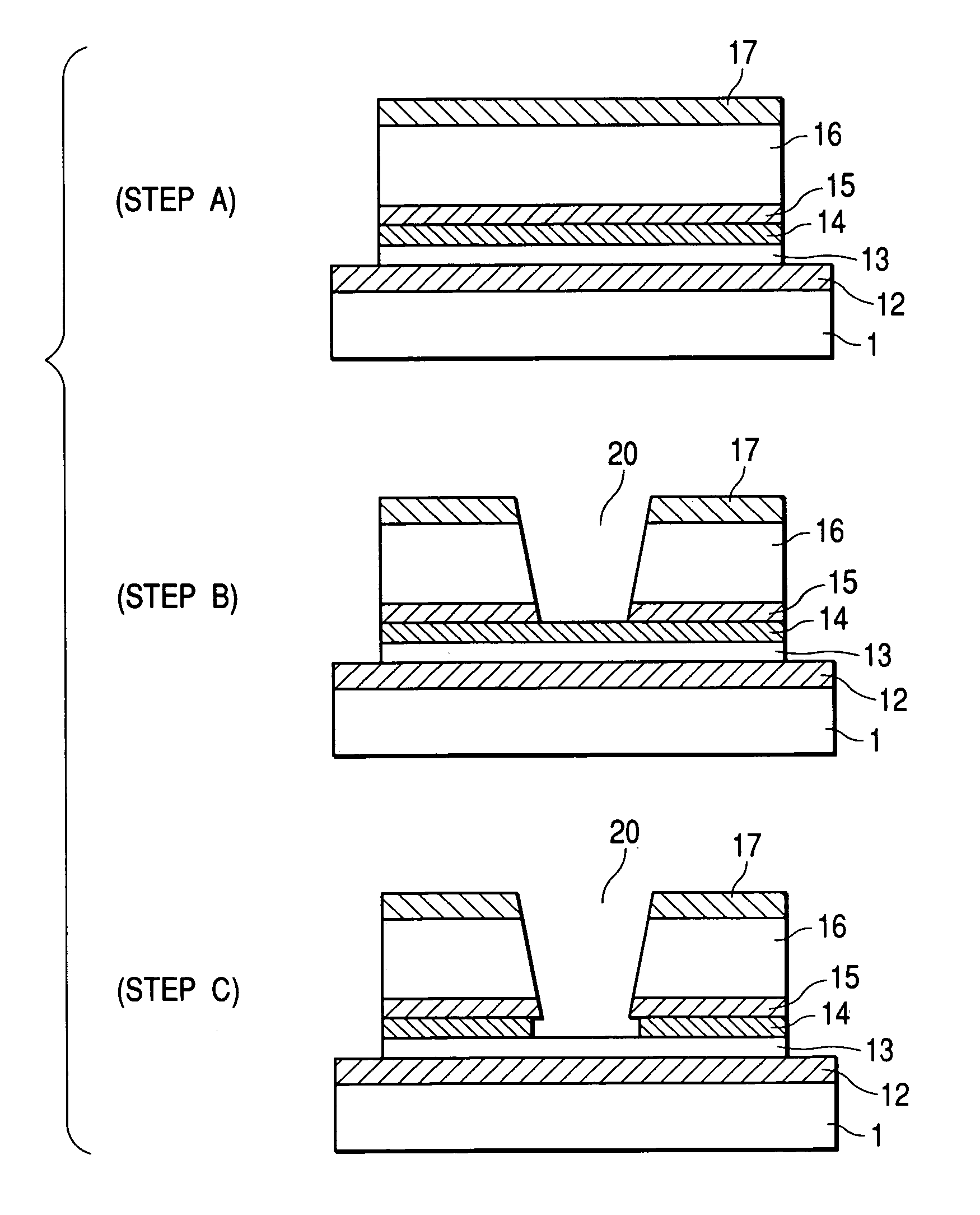
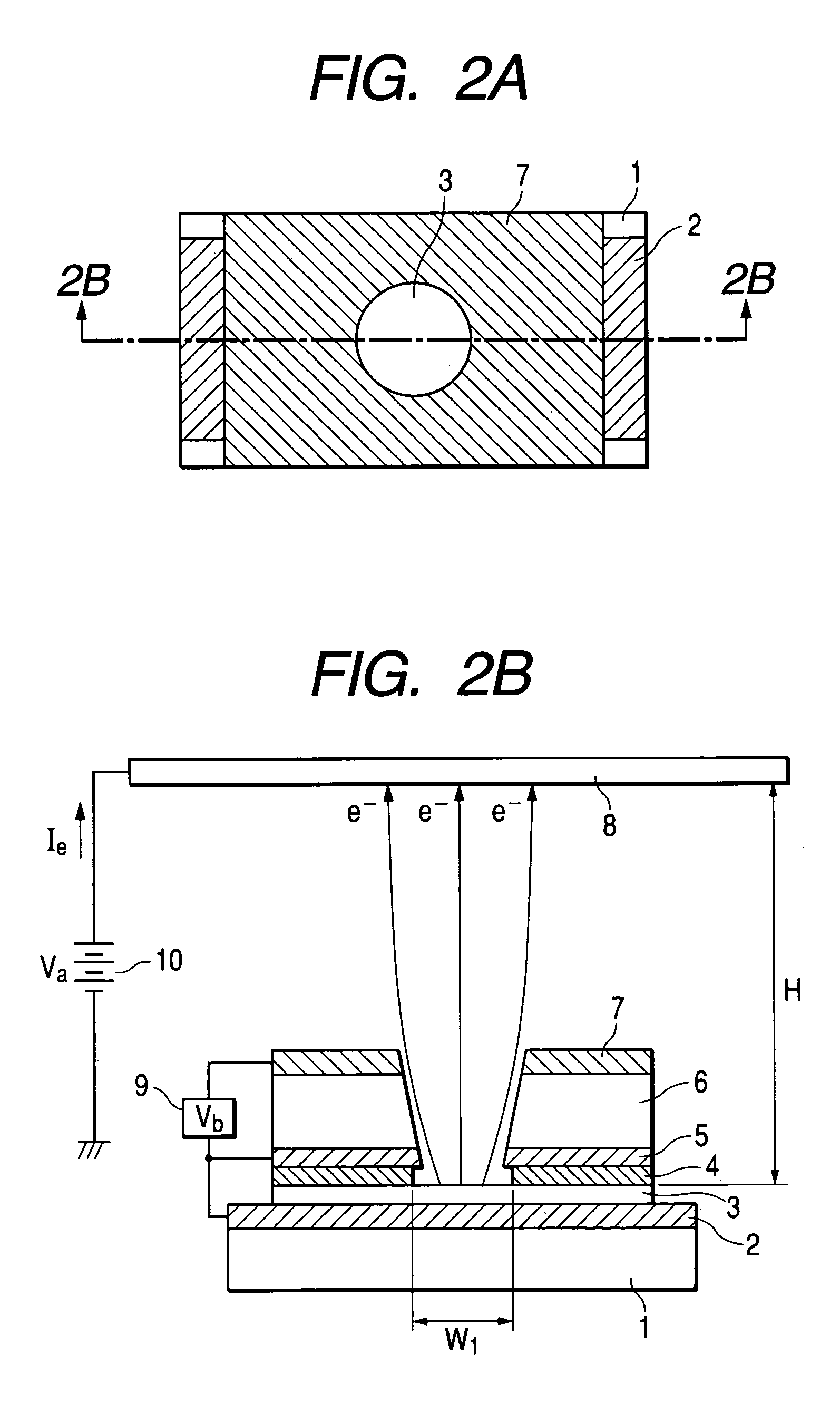
[0072]An electron-emitting device having the structure shown in FIGS. 2A and 2B was manufactured according to the steps shown in FIG. 3.

[0073](Step 1)

[0074]The substrate 1 made of quartz was used and sufficiently washed, and then an Al film having a thickness of 300 nm was formed as the first electroconductive layer 12 on the substrate 1 by a sputtering method.

[0075](Step 2)

[0076]A diamond-like carbon film was deposited on the first electroconductive layer 12 at about 30 nm by using plasma CVD method to obtain the electron-emitting film 3.

[0077](Step 3)

[0078]A Cr film was formed as the protective layer 14 on the layer 13 containing at least one of materials composing the electron-emitting element by a sputtering method such that a thickness of the Cr film becomes 50 nm.

[0079](Step 4)

[0080]A Ta film was formed as the second electroconductive layer 15 on the protective layer 14 such that a thickness of the Ta film became 50 nm.

[0081](Step 5)

[0082]In order to form the insulating layer ...

example 2

[0093]An electron-emitting device having the structure shown in FIGS. 2A and 2B was manufactured according to the steps shown in FIG. 3.

[0094](Step 1)

[0095]The substrate 1 made of quartz was used and sufficiently washed, and then a Pt film having a thickness of 300 nm was formed as the first electroconductive layer 12 on the substrate 1 by a sputtering method.

[0096](Step 2)

[0097]A diamond-like carbon film was deposited on the first electroconductive layer 12 at about 100 nm by using plasma CVD method to obtain the electron-emitting film 3.

[0098](Step 3)

[0099]In order to form the protective layer 14, an SiO2 film was formed at about 50 nm by plasma CVD method using SiH4 and O2 as raw gases.

[0100](Step 4)

[0101]A Cr film having a thickness of 50 nm was formed as the second electroconductive layer 15 on the protective layer 14 by a sputtering method.

[0102](Step 5)

[0103]In order to form the insulating layer 16, an SiO2 film was formed at about 1000 nm by plasma CVD method using SiH4 and ...

example 3

[0113](Step 1)

[0114]The substrate 1 made of quartz was used and sufficiently washed, and then a Pt film having a thickness of 300 nm was formed as the first electroconductive layer 12 on the substrate 1 by a sputtering method.

[0115](Step 2)

[0116]A large number of Co particles (catalytic, particles) were deposited for the layer 13 containing at least one of materials composing the electron-emitting element on the first electroconductive layer 12 by a sputtering method.

[0117](Step 3)

[0118]In order to form the protective layer 14, an SiO2 film was formed at about 50 nm by plasma CVD method using SiH4 and O2 as raw gases.

[0119](Step 4)

[0120]A Cr film having a thickness of 50 nm was formed as the second electroconductive layer 15 on the protective layer 14 by a sputtering method.

[0121](Step 5)

[0122]In order to form the insulating layer 16, an SiO2 film was formed at about 1000 nm by plasma CVD method using SiH4 and O2 as raw gases.

[0123](Step 6)

[0124]A Ta film was formed by resistance he...


PUM


Abstract

A method of manufacturing an electron-emitting device, which has an easy manufacturing process and preferably controls an electron beam diameter. The method includes: arranging on a substrate a member comprising a first electroconductive layer blanketing the substrate, a layer containing at least one of materials forming an electron-emitting element blanketing the first electroconductive layer, a protective layer blanketing the layer containing at least one of materials, a second electroconductive layer blanketing the protective layer, an insulating layer blanketing the second electroconductive layer, and a third electroconductive layer blanketing the insulating layer; forming an opening, which extends from a surface of the third electroconductive layer to the protective layer, by dry etching; and wet-etching the protective layer through the opening to expose a portion of the layer containing at least one of the materials forming the electron-emitting element.

Description

BACKGROUND OF THE INVENTION[0001]1. Field of the Invention[0002]The present invention relates to a method of manufacturing an electron-emitting device, a method of manufacturing an electron source, and a method of manufacturing an image display device.[0003]2. Related Background Art[0004]An electron-emitting device includes a field emission type (hereinafter referred to as FE-type) electron-emitting device and a surface conduction type electron-emitting device.[0005]With respect to the FE-type electron-emitting device, a spindt type is expected because of high efficiency. However, a process for manufacturing a spindt type electron-emitting device is complicated and an electron beam is easily dispersed. Therefore, in order to prevent the spread of the electron beam, it is necessary to arrange a focusing electrode above an electron-emitting region.[0006]On the other hand, with respect to an example of an electron-emitting device having an electron beam diameter smaller than the spindt...

Claims


Application Information

Patent Timeline
IPC IPC(8): H01J9/00H01J1/30H01J9/02
CPCH01J9/025H01J1/304H01J1/3042H01J2329/0444H01J2329/046
Inventor TERAMOTO, YOJI
Owner CANON KK
Why Eureka
Try Eureka