Light emitting component comprising organic layers

a technology of light emitting components and organic layers, which is applied in the direction of discharge tubes luminescnet screens, instruments, natural mineral layered products, etc., can solve the problems of poor conductivity and mobility of charge-carrier transport layers, failure to advance this approach, and low transparency, so as to achieve greater homo distance between transport layers and emitters. , the effect of ionization potential

Inactive Publication Date: 2006-07-11
NOVALED GMBH
View PDF9 Cites 266 Cited by
  • Summary
  • Abstract
  • Description
  • Claims
  • Application Information

AI Technical Summary

Benefits of technology

[0037]In this respect, this approach clearly differs from that presented in the patent of Ogura et al., EP 1,017,118 A2. None of the examples listed in this reference meets the above conditions. Accordingly, the light-emitting diodes disclosed therein are also clearly poorer with respect to operating voltage as well as to efficiency than the examples of the present invention. The blocking layer proposed in patent EP 1,017,118 A2 acts only to prevent the injection of minority charge carriers. This function can also be satisfied by the blocking layer of the present invention, which in addition meets the condition that minority charge carriers are efficiently arrested at the light-emitting layer / blocking layer interface.

Problems solved by technology

Further research, however, has failed to advance this approach.
The reason for this is believed to be due to the poor injection of charge carriers from the contacts into organic layers and in the comparatively poor conductivity and mobility of charge-carrier transport layers.
However, the extreme instability and reactivity of the corresponding metals, and the low transparency of these contact materials undercut this potential remedy.
In practice, therefore, at this time indium tin oxide (ITO) is used almost exclusively as the injection contact for holes (a transparent degenerate semiconductor), whose work function, however, is still too limited.
However, such materials are hard to dope, since extremely strong acceptors and donors would be required, so that these conditions cannot be fully met on both sides with materials that are actually available.
In addition, the problem of exciplex formation becomes more acute when doped HTLs and ETLs are used, since in doped materials the Debye shielding length is very small and hence high charge-carrier thicknesses occur directly at the interface.
In addition, dopants in the immediate vicinity of the EL may result in quenching of fluorescence by, for example, Förster transfer.
The basic dilemma, that materials with deep-lying HOMO are hard to p-dope, but materials with high-lying HOMO promote exciplex formation at the interface to the emitting layer, has not yet been recognized in the scientific literature.

Method used


Image

  • Light emitting component comprising organic layers
  • Light emitting component comprising organic layers
  • Light emitting component comprising organic layers

Examples


Embodiment Construction

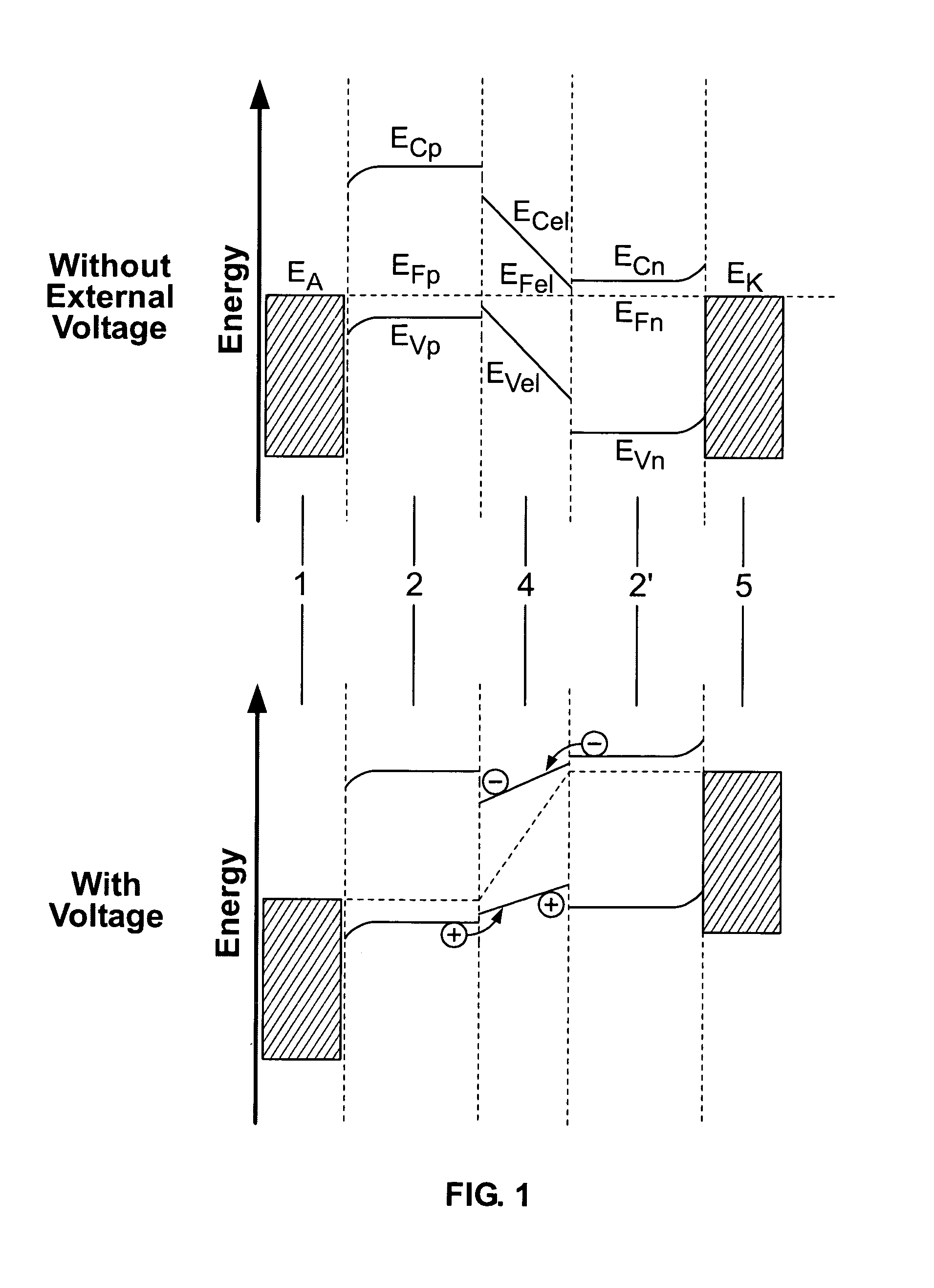
[0066]A theoretically ideal structure is represented in FIG. 1, comprising an anode (EA), a highly p-doped hole-injection and transport layer (EVp, ECp, EFp), an electroluminescent layer (EVel, ECel, EFel), a highly n-doped electron-injecting and transporting layer (EVn, ECn, EFn), and a cathode. When voltage is applied (anode polarized positively), holes from the anode and electrons from the cathode are injected in the direction of the light-emitting layer. Since no barrier occurs (EVp>EVel) either for holes at the interface of the p-doped layer to the light-emitting layer, or for electrons at the interface of the n-doped layer to the light-emitting layer (ECn>ECel), and a high barrier exists (ECelCp and EVel>EVp) at the interface of the light-emitting layer to the p-doped and n-doped layer for electrons and holes respectively, the charge carriers (electrons and holes) collect in the light-emitting layer, where they can efficiently form excitons and recombine radiantly. In reality,...


PUM

PropertyMeasurementUnit
thicknessaaaaaaaaaa
thicknessesaaaaaaaaaa
luminescenceaaaaaaaaaa

Abstract

The invention relates to a light-emmiting component having organic layers, in particular to an organic light-emmiting diode. The component has at least one doped charge carrier transport layer (2), a light-emmiting layer (4) and contact layers (1, 5) and also has a blocking layer (3; 3′) wherein an organic material is provided between the charge carrier transport layer (2, 2′) and the light-emmiting layer (4). The energy levels of the charge carried transport layer are chosen in such a way that efficient doping is possible and the blocking layer nevertheless ensures that non-radiating recombination processes on the interface with the emitting layer are prevented.

Description

CROSS-REFERENCE TO RELATED APPLICATIONS[0001]This is a national application for International Application No. PCT / DE01 / 04422 which was filed on Nov. 20, 2001, and which published in German on May 23, 2002, which in turn claims priority from 100 58 578.7, which was filed on Nov. 20, 2000.[0002]The invention relates to a light-emitting component comprising organic layers, including a blocking layer of organic material between a charge-carrier transport layer and a light-emitting layer.BACKGROUND OF THE INVENTION[0003]Since the demonstration of low operating voltages by Tang et al., 1987 [C. W. Tang et al. Appl. Phys. Lett. 51 (12) 913 (1987)], organic light-emitting diodes have been promising candidates for the realization of large-area displays. They consist of a sequence of thin (typically 1 nm to 1 μm) layers of organic materials, which preferably are produced by vacuum deposition or by spin-on deposition in their polymer form. After electrical contacting by metallic layers they fo...

Claims


Application Information

Patent Timeline
Patent Type & Authority Patents(United States)
IPC IPC(8): H05B33/12H01L51/50
CPCH01L51/5012H01L51/5052H01L51/5096Y10T428/26Y10S428/917H10K50/155H10K50/165H10K50/18H10K50/11H05B33/22
Inventor PFEIFFER, MARTINLEO, KARLBLOCHWITZ-NIEMOTH, JANZHOU, XIANG
Owner NOVALED GMBH
Why Eureka
Try Eureka