Liquid crystal display device and light emitting structure with photonic band gap transparent electrode structures

a transparent electrode and liquid crystal display technology, applied in the field of liquid crystal display devices and light emitting structures, can solve the problems of reducing the voltage signal level and the electrical current required, reducing the power consumption of the lcd device, etc., and achieves the effect of increasing the responsiveness or speed of the transparent electrode, increasing the conductivity, and increasing the conductivity

Inactive Publication Date: 2006-07-11
GOVERNMENT OF THE UNITED STATES SEC OF THE ARMY DEPT OF THE ARMY - OFFICE OF THE SEC +1
View PDF10 Cites 22 Cited by
  • Summary
  • Abstract
  • Description
  • Claims
  • Application Information

AI Technical Summary

Benefits of technology

[0018]A conductivity of the transparent metal stack of the present invention when all of the metal layers in the metal stack are contacting one another is advantageously 100 to 1000 times greater than a conductivity of conventional semiconductor/metal-oxide transparent materials, such as ITO. The dramatic increase in conductivity arises from the alternating metal layers included in the transparent metal stack. While the transparent metal stack provides a required transparency to light, the dramatic increase in conductivity associated therewith over conventional transparent semiconductor/metal-oxide materials advantageously results in a substantial corresponding increase in a responsiveness or speed of the transparent electrode, and thus the LCD

Problems solved by technology

Also, the substantial increase in the transparent electrode conductivity advantageously results in a decrease in the voltage signal level

Method used


Image

  • Liquid crystal display device and light emitting structure with photonic band gap transparent electrode structures
  • Liquid crystal display device and light emitting structure with photonic band gap transparent electrode structures
  • Liquid crystal display device and light emitting structure with photonic band gap transparent electrode structures

Examples


Embodiment Construction

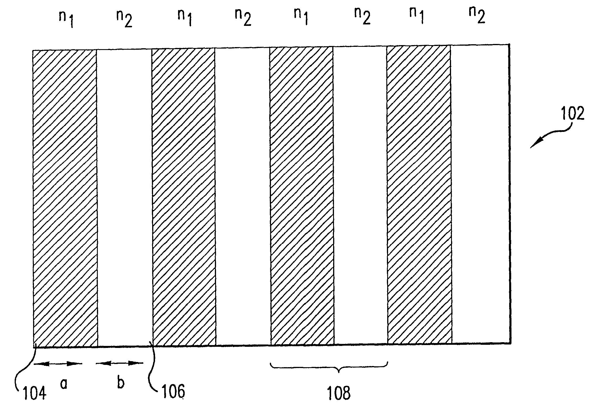
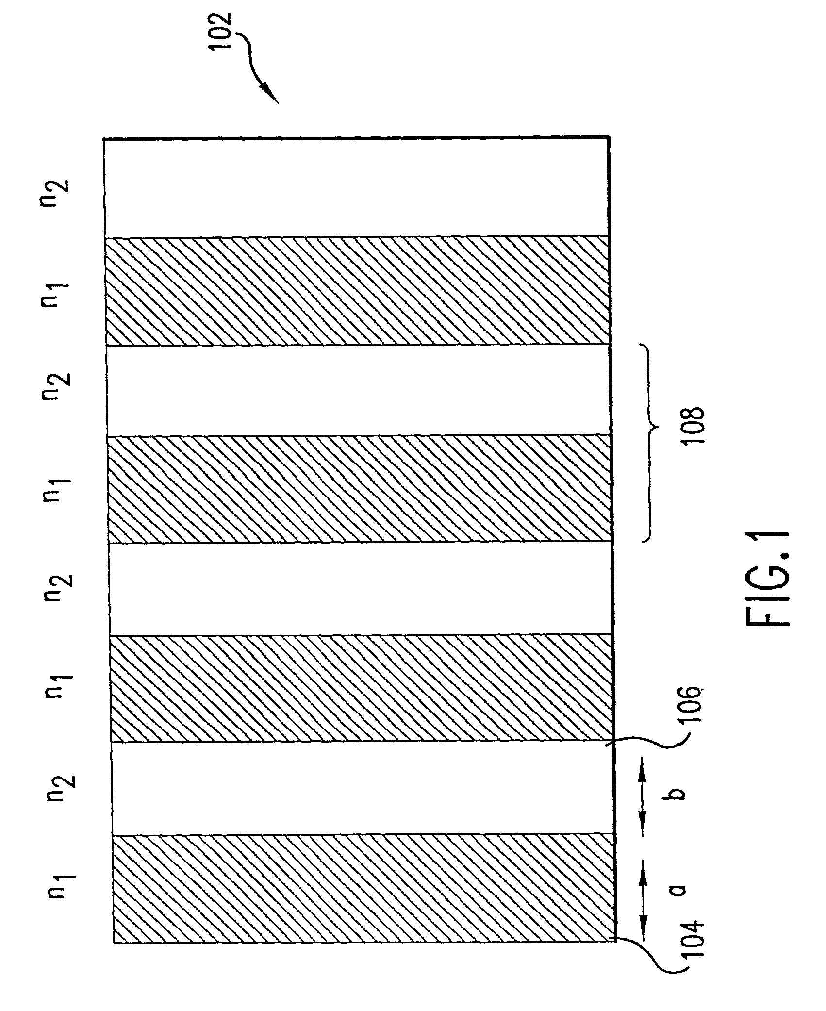
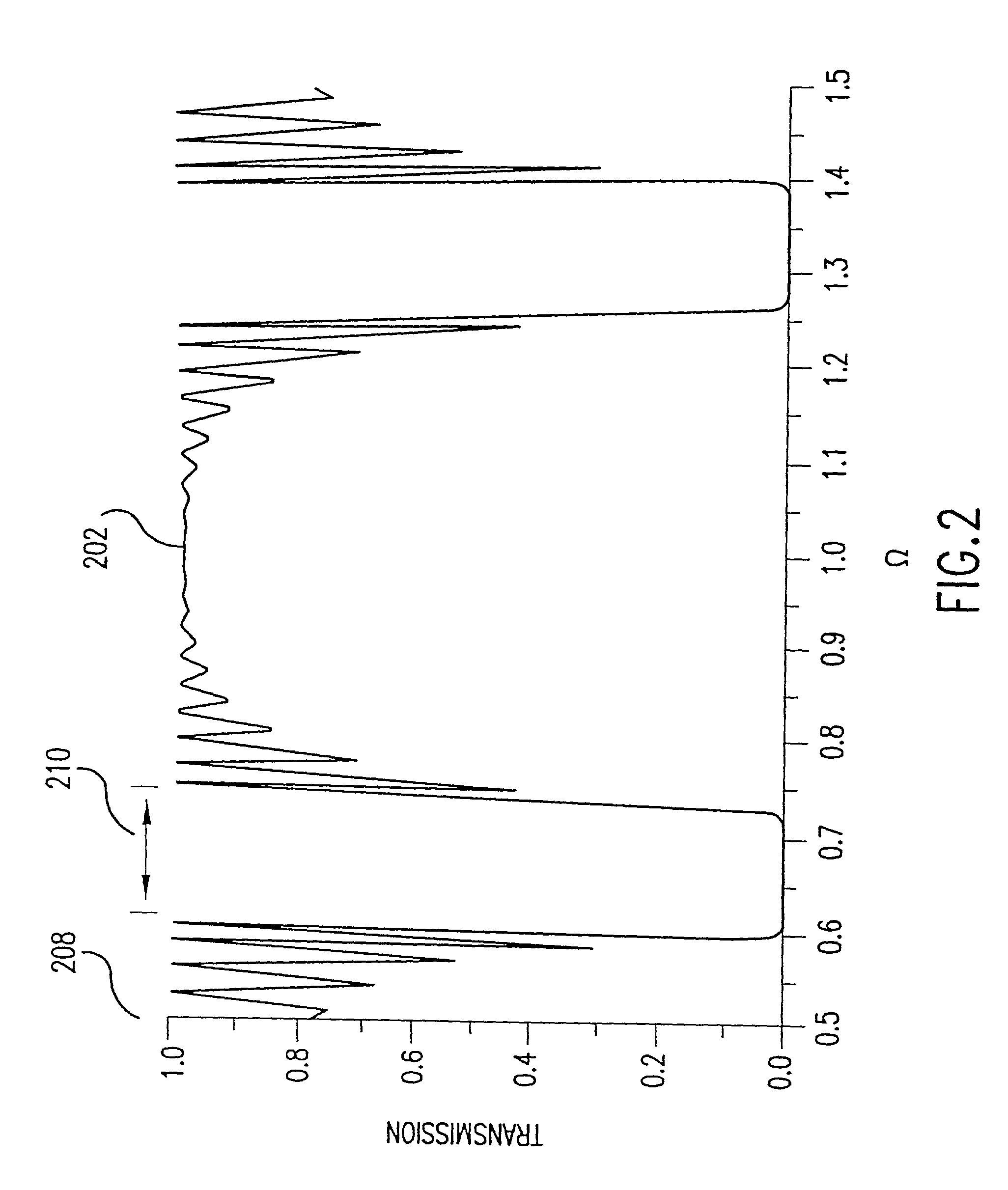
[0043]I. Photonic Band Gap (PBG) Structures[0044]A. An Example PBG Structure[0045]B. Transmission and Reflection Properties of Metallic Structures[0046]C. Transparent Metal PBG Structures[0047]D. Experimental Results of a Transparent Metal PBG Photonic Device[0048]II. Liquid Crystal Displays (LCDs) with PBG Transparent Electrode Structures[0049]A. A Basic LCD Device[0050]B. An Active Matrix LCD Device[0051]C. A Passive Matrix LCD Device[0052]D. Conclusion[0053]III. Light Emitting Structures[0054]A. Prior Art Light Emitting Diode[0055]B. Light Emitting Structures with PBG Transparent Metal Electrode

[0056]In the present invention, a transparent, multilayered electrode, or transparent metal stack, exhibiting a photonic band gap structure that transmits a visible range of wavelengths and suppresses a non-visible range of wavelengths of the electromagnetic spectrum, replaces a conventional transparent electrode made of a transparent semiconductor / metal-oxide, such as ITO, in an LCD devic...


PUM


Abstract

An LCD device for displaying an image includes pixel control electrodes constructed as a transparent metal stack having a photonic band gap (PBG) structure that transmits a visible range of wavelengths and suppresses a non-visible range of wavelengths. A liquid crystal layer between the pixel control electrodes controls the transmission of light in response to a voltage applied across the pixel control electrodes. A light emitting structure (LES), such as a light emitting diode (LED) or light emitting polymer (LEP) device includes a cathode electrode, a substrate, an active layer for emitting visible light, and a transparent anode electrode having a PBG structure.

Description

CROSS-REFERENCE TO RELATED APPLICATIONS[0001]This application is a continuation-in-part of “Transparent Metallo-Dielectric Photonic Band Gap Structure,” Ser. No. 08 / 931,756, by M. Scalora, filed on Sep. 16, 1997, now issued as U.S. Pat. No. 6,262,830 on Jul. 17, 2001 (incorporated by reference in its entirety herein), and claims the benefit of U.S. Provisional Application No. 60 / 186,762, filed Mar. 3, 2000.FEDERALLY SPONSORED RESEARCH AND DEVELOPMENT[0002]This invention was made with Government support under Contract DAAH01-96-P-R010 awarded by the U.S. Army Missile Command. The Government has certain rights in the invention.BACKGROUND OF THE INVENTION[0003]1. Field of the Invention[0004]This invention relates generally to liquid crystal display (LCD) devices and light emitting structures (LESs), such as light emitting diodes (LEDs) and light emitting polymer (LEP) devices.[0005]2. Related Art[0006]Liquid Crystal Displays are used in many practical display systems including display ...

Claims


Application Information

Patent Timeline
IPC IPC(8): G02F1/1343G02B6/122H01L33/00H01L51/50H01L51/52
CPCB82Y20/00G02B6/1225G02F1/13439H01L51/5036H01L51/5206H01L51/5262G02F2202/32H10K50/125H10K50/816H10K50/85H10K50/858
Inventor SCALORA, MICHAELBLOEMER, MARK
Owner GOVERNMENT OF THE UNITED STATES SEC OF THE ARMY DEPT OF THE ARMY - OFFICE OF THE SEC
Why Eureka
Try Eureka