Supercharge Your Innovation With Domain-Expert AI Agents!

Apparatus and methods for compensating plasma sheath non-uniformities at the substrate in a plasma processing system

a plasma processing system and substrate technology, applied in the direction of electrical apparatus, emergency protective arrangement details, electric discharge tubes, etc., can solve the problems of increasing the diameter of the sidewall, reducing the uniformity of plasma density distribution, and adding significant cost to the manufacture of the plasma processing system, so as to reduce the impact of overall system cost, minimize development and manufacturing costs, and improve the radial uniformity of substrate plasma processing

Inactive Publication Date: 2006-07-11
TOKYO ELECTRON LTD
View PDF61 Cites 11 Cited by
  • Summary
  • Abstract
  • Description
  • Claims
  • Application Information

AI Technical Summary

Benefits of technology

[0008]In one aspect, the invention relates to a method to compensate for radial non-uniformity of a plasma-related parameter at a substrate-supporting surface of an electrostatic chuck. The method includes characterizing the radial non-uniformity in the plasma-related parameter and selecting a compensating structure having a specific capacitance for capable of substantially compensating for the radial non-uniformity in the plasma-related parameter. The presence of the compensating structure makes the effective specific capacitance uniform over the extent of the substrate-supporting surface. The substrate-supporting surface is modified for providing a pattern of features characteristic of the compensating structure and then covered conformally with a planarization coating of a dielectric material. The dielectric material fills the pattern of features to provide the compensating structure.
[0010]In accordance with the principles of the invention, radial non-uniformities in the plasma sheath, and hence a plasma-related parameter, are compensated adjacent to the substrate-supporting surface over the area of the substrate-supporting surface or, at the least, over an area of at least the size of a substrate being processed. The radial uniformity of substrate plasma processing is improved with a minimal impact on the overall system cost as the only system modifications are to the electrostatic chuck holding the substrate. For example, the principles of the invention may be implemented in a plasma processing system without modifying other elements of the system design, such as the RF generator, antenna or matching unit. The improvement in the plasma-related parameter is achieved without deviating significantly from developed processes and technology, which minimizes developmental and manufacturing costs associated with implementing the principles of the invention.
[0011]The compensating structures of the invention may be used in any ICP plasma processing system for improving the uniformity of the plasma-surface interaction on the substrate for conventional processes, such as plasma etching, sputtering, deposition, and cleaning. Compensating structures of dielectric material fabricated in accordance with the principles of the invention can be applied to any surface in a plasma processing system that is exposed to the plasma, such as the chamber walls and deposition shields, for controlling the uniformity of the plasma-surface interaction with the plasma-exposed surface.

Problems solved by technology

Although these techniques improve the uniformity of the plasma density distribution, the contribution of the chamber sidewall to the radial decrease in the plasma density distribution remains unaffected.
Increasing the diameter of the sidewall lessens the radial non-uniformity but adds significant cost to the manufacture of the plasma processing system.
Attempts have been made to compensate sidewall effects by increasing the dimensions of the ICP source dielectric window, which must be robust and thus expensive, and by adding control units, power supplies, and cooling systems, which also adds hardware complexity.
In plasma processing systems for large dimension substrates, such corrective measures increase material and consumables expenses, add complexity, and result in an increased cost of operation.
As a result, the overall cost of the plasma processing system is significantly increased.

Method used


Image

  • Apparatus and methods for compensating plasma sheath non-uniformities at the substrate in a plasma processing system
  • Apparatus and methods for compensating plasma sheath non-uniformities at the substrate in a plasma processing system
  • Apparatus and methods for compensating plasma sheath non-uniformities at the substrate in a plasma processing system

Examples


Embodiment Construction

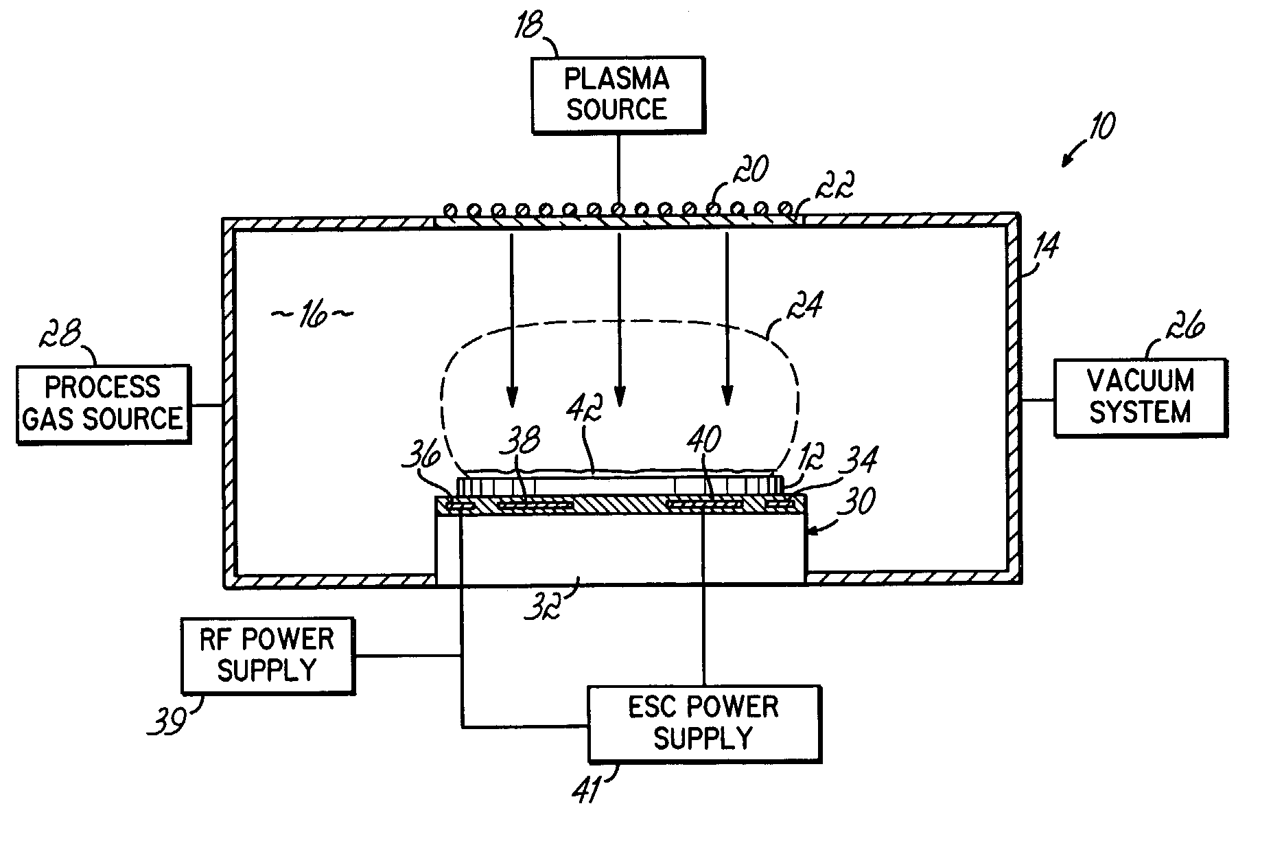
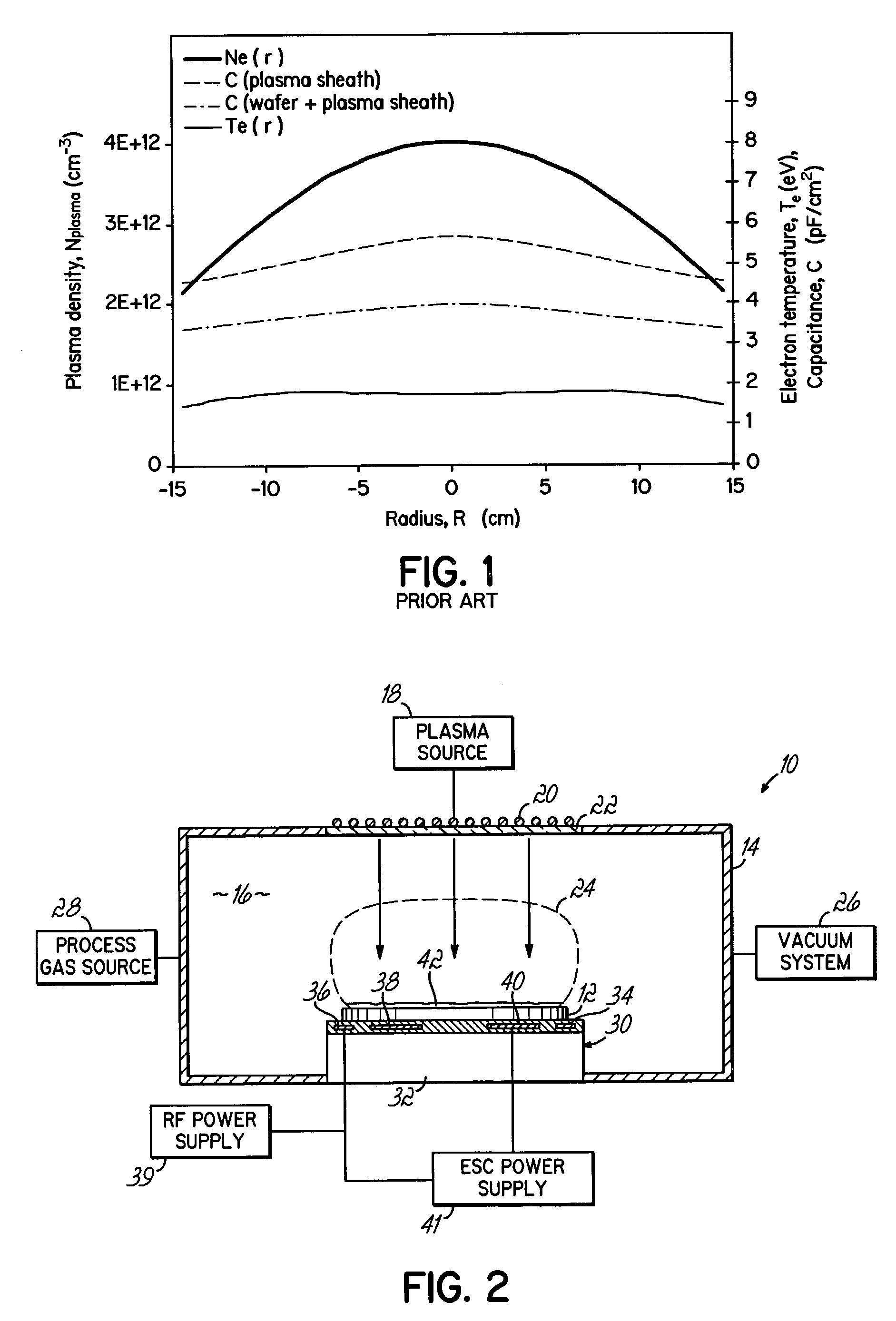
[0037]With reference to FIG. 2, a plasma processing system 10 operable for treating a substrate 12, such as a semiconductor wafer, with an inductively-coupled plasma (ICP) is depicted. Processing system 10 includes a processing chamber 14 that encloses a processing space 16 with a grounded sidewall. The processing system 10 is provided with a plasma power source 18 electrically connected in a known manner to an antenna 20 positioned adjacent to a planar dielectric window 22, which forms a sealed portion of the processing chamber 14. The plasma power source 18 conventionally includes a radio-frequency (RF) power supply and appropriate RF matching circuitry adapted for efficient coupling of RF power, typically at 13.56 MHz, to the antenna 20. Antenna 20 directs RF power through the dielectric window 22 into the processing space 16 for generating and sustaining a plasma 24 in processing space 16 by interacting with a rarified atmosphere of a partial pressure of process gas, such as arg...


PUM


Abstract

Apparatus and methods to compensating for radial non-uniformities in the plasma sheath at a substrate held by an electrostatic chuck in a plasma processing system. The substrate is held by a substrate-supporting surface of the electrostatic chuck. The substrate-supporting surface is modified by providing a pattern of features characteristic of a compensating structure that corrects the radial non-uniformities in the plasma sheath and then covering the features conformally with a planarization coating of a dielectric material. The dielectric material fills and covers the pattern of features to provide multiple parallel capacitances defining the compensating structure. The pattern of features characterizing the compensating structure may be determined from a radial non-uniformity in a plasma-related parameter at the substrate-supporting surface.

Description

FIELD OF THE INVENTION[0001]This invention relates to plasma processing systems and, in particular, to electrostatic chucks for plasma processing systems that improve the plasma sheath uniformity at the substrate-supporting surface of the chuck.BACKGROUND OF THE INVENTION[0002]Electrostatic chucks are used for securing substrates, such as semiconductor wafers, in vacuum chambers of plasma processing systems. Generally, an electrostatic chuck includes a dielectric body and one or more electrodes embedded within the dielectric body. A chucking voltage applied to the electrodes establishes a clamping force by operation of Coulomb's law. The clamping force attracts the substrate toward a wafer-supporting surface of the dielectric body and holds the backside of the substrate in contact with the wafer-supporting surface. The exposed surface of the clamped substrate is subjected to a plasma process including, but not limited to, plasma cleaning, plasma etching, and plasma-enhanced depositi...

Claims


Application Information

Patent Timeline
Patent Type & Authority Patents(United States)
IPC IPC(8): H02H1/00H01J37/32H01L21/00H01L21/683
CPCH01J37/32623H01L21/6833H01L21/67069
Inventor BRCKA, JOZEF
Owner TOKYO ELECTRON LTD
Features
  • R&D
  • Intellectual Property
  • Life Sciences
  • Materials
  • Tech Scout
  • Unparalleled Data Quality
  • Higher Quality Content
  • 60% Fewer Hallucinations
Learn More