Semiconductor device for controlling switching power supply

a technology of switching power supply and semiconductor device, which is applied in the direction of electric variable regulation, process and machine control, instruments, etc., can solve the problems of increasing the cost of the overall circuit including the semiconductor device for controlling the switching power supply, reducing the current, and reducing so as to reduce the current loss of the switching element at light load, reduce power consumption, and achieve high power efficiency

Inactive Publication Date: 2006-07-11
PANASONIC CORP
View PDF6 Cites 35 Cited by
  • Summary
  • Abstract
  • Description
  • Claims
  • Application Information

AI Technical Summary

Benefits of technology

[0023]The present invention is devised to solve the conventional problems. An object of the present invention is to provide a semiconductor device for controlling a switching power supply whereby the current loss of a switching element at light load can be reduced to further reduce power consumption at light load, sufficiently high power efficiency can be readily obtained over a wide load area including a standby mode, and the efficiency of the switching power supply can be further improved at low cost.
[0027]As described above, according to the present invention, during the stop period of the intermittent operation, a comparison is made between the number of counts of the waveform of the transformer reset detection signal and a set count value having been set in the counter circuit. When a return control signal is outputted from the light load detection circuit before there is a match, control is performed to turn on the switching element according to the timing of the waveform of the transformer reset detection signal after the return control signal is outputted, thereby reducing a switching power loss caused by a resonant capacitor during an intermittent switching operation at light load.
[0028]For this reason, it is possible to reduce a current loss of the switching element under light load to further reduce power consumption under light load, to readily obtain sufficiently high power efficiency over a wide load area including a standby mode, and to further improve the efficiency of the switching power supply at low cost.

Problems solved by technology

However, this power supply system requires two switching power supply units (converters), increasing the cost of the overall circuit including the semiconductor devices for controlling the switching power supplies.
Therefore, it is not possible to reduce a current flowing to the switching power supply to 0 as well as a current flowing to the switching element and thus a certain amount of current is applied even at no load.
Hence, the switching operation of the switching element causes a loss even at no load and a lighter load causes a larger loss in the switching element.
Consequently, the switching power supply decreases in power efficiency and thus it is not possible to meet the need for lower power consumption in a standby state of the power supply.
Further, the switching power supply of partial resonance has the following problem: since the switching power supply has a high oscillation frequency at light load, a switching loss increases and the efficiency of the power supply decreases in a standby mode.
Thus, improvement in the efficiency of the power supply during standby is still insufficient.
Further, since an intermittent switching operation is performed by intermittent oscillation control at light load, it is possible to suppress an increase in switching frequency, which generally causes a problem in RCC, at light load.
It is not possible to recognize the level of the drain voltage of the switching element when switching is restarted by the return signal, resulting in hard switching at the restart of switching.
Thus, a switching loss occurs when the switching element is turned on.
For these reasons, it is not possible to reduce the current loss of the switching element at light load or obtain sufficiently high power efficiency over a wide load area including a standby mode, thereby interfering with low cost and improvement in the efficiency of the switching power supply.

Method used


Image

  • Semiconductor device for controlling switching power supply
  • Semiconductor device for controlling switching power supply
  • Semiconductor device for controlling switching power supply

Examples


embodiment 1

[0046]A semiconductor device for controlling a switching power supply will be discussed below according to Embodiment 1 of the present invention.

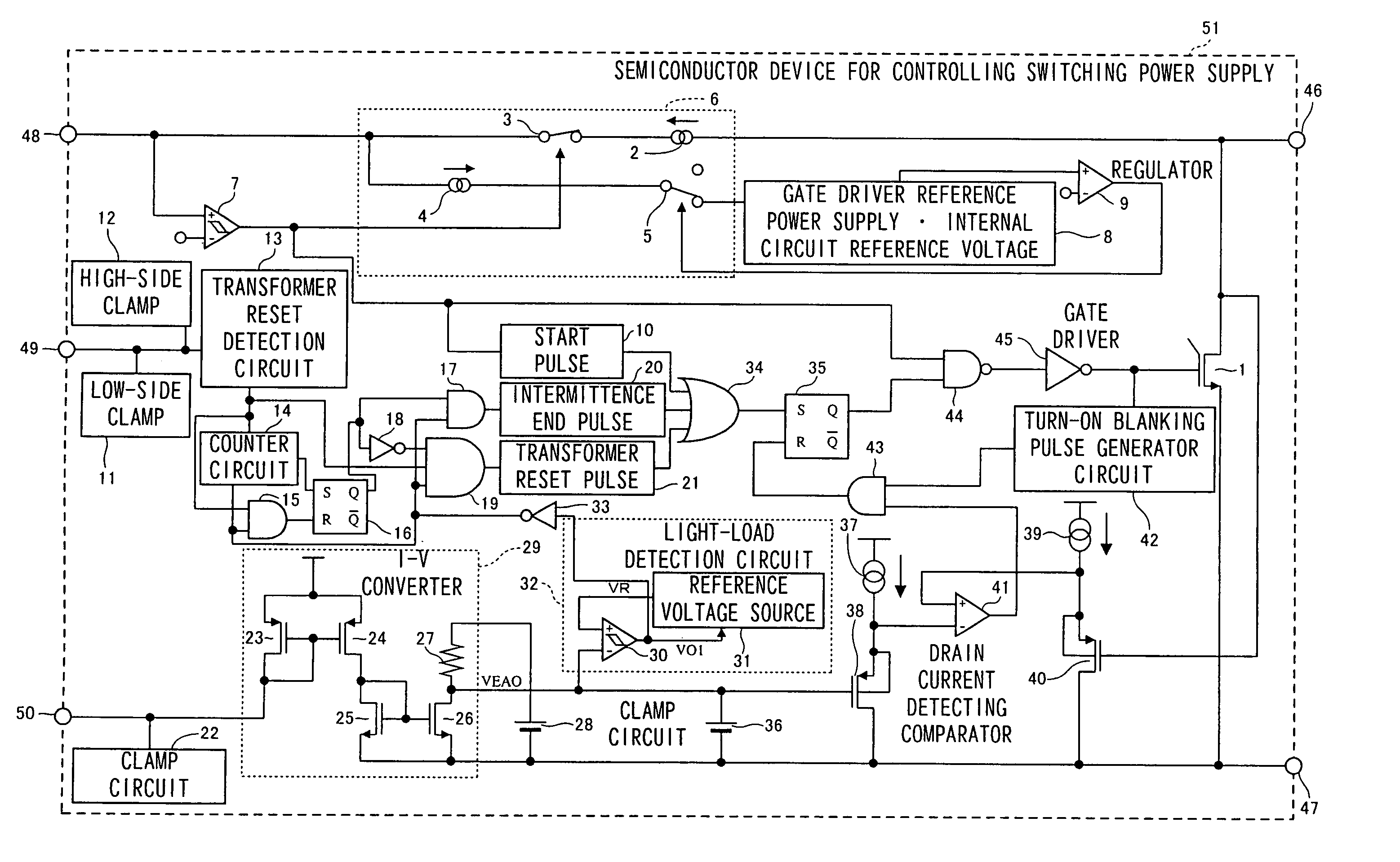
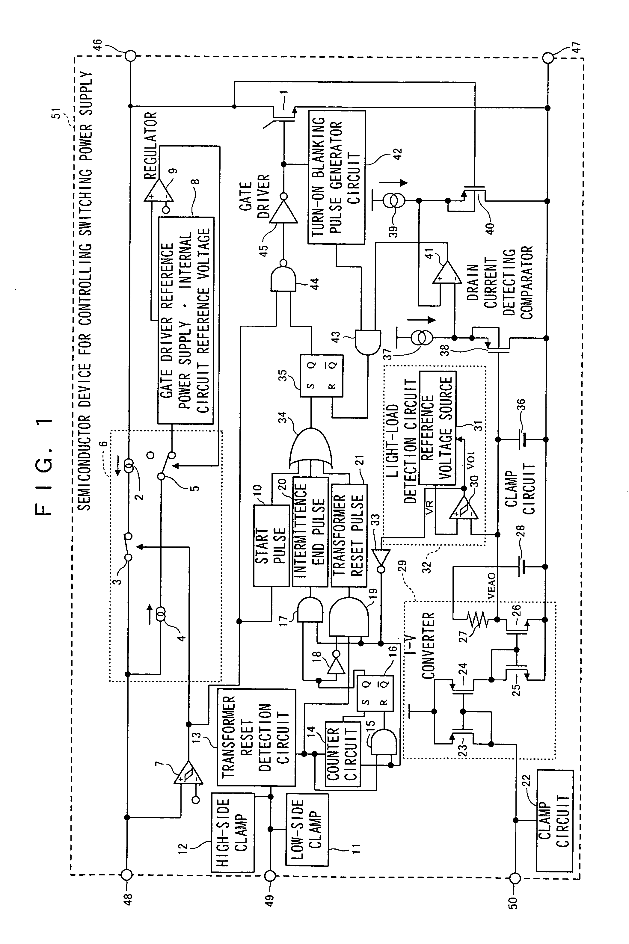
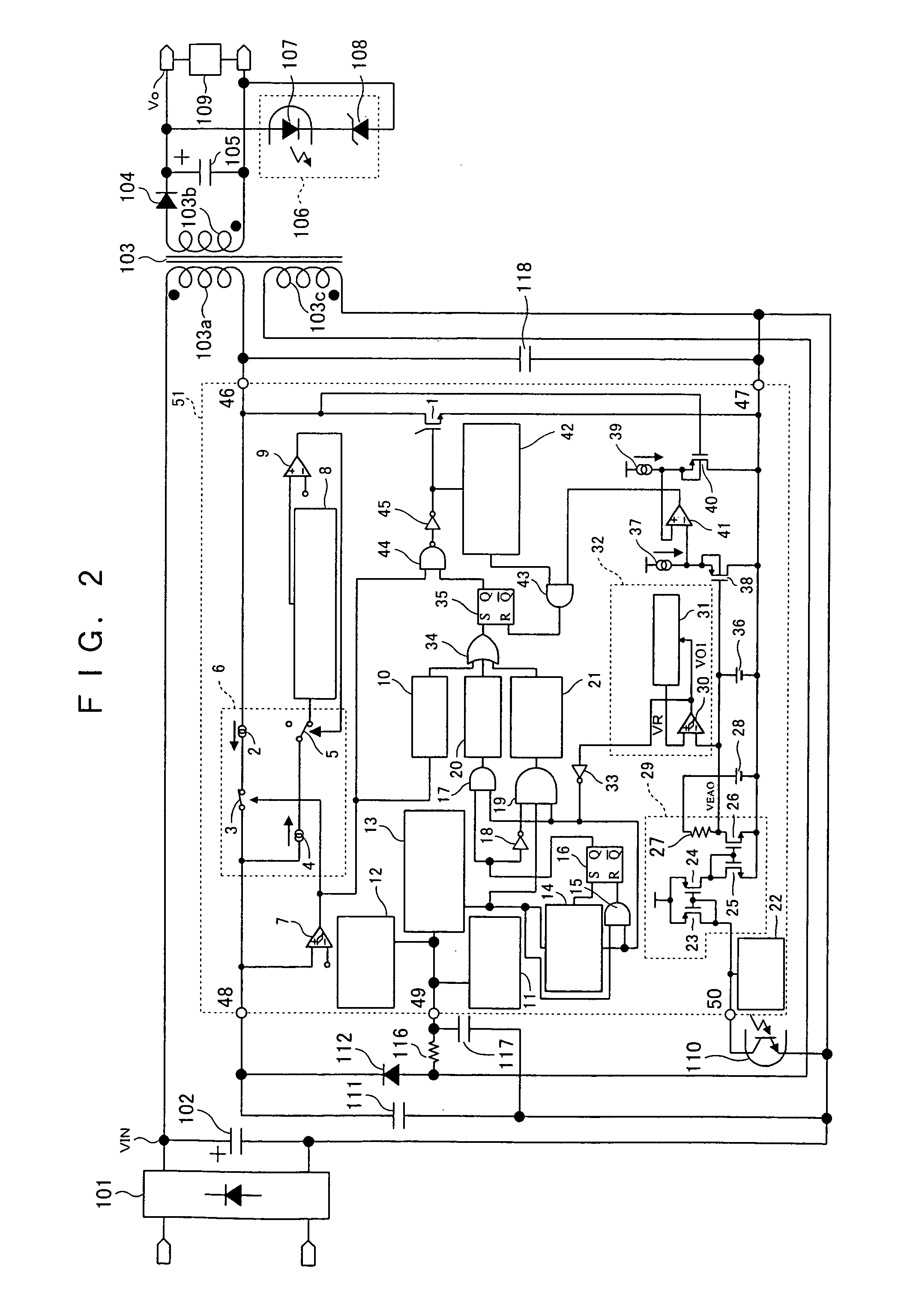
[0047]FIG. 1 is a circuit diagram showing a structural example of the semiconductor device for controlling the switching power supply according to Embodiment 1. FIG. 2 is a circuit diagram showing a structural example of the switching power supply configured using the semiconductor device for controlling the switching power supply according to Embodiment 1.

[0048]In a semiconductor device 51 for controlling a switching power supply, a switching element 1 including a power MOSFET and a control circuit for performing switching control on the switching element 1 are integrated on the same semiconductor substrate. The semiconductor device 51 is constituted of five terminals: an input terminal 46 and an output terminal 47 of the switching element 1, a starting voltage detecting terminal of the semiconductor device 51 for controlling the switching...

embodiment 2

[0105]A semiconductor device for controlling a switching power supply will be discussed below according to Embodiment 2 of the present invention.

[0106]FIG. 9 is a circuit diagram showing a structural example of a semiconductor device for controlling a switching power supply according to Embodiment 2. FIG. 10 is a waveform chart showing a switching operation in the semiconductor device for controlling the switching power supply according to Embodiment 2. FIG. 11 is a circuit diagram showing a structural example of a delay circuit in the semiconductor device for controlling the switching power supply according to Embodiment 2.

[0107]FIG. 9 shows that a delay circuit 52 is added to FIG. 1. The following will discuss the meaning of the delay circuit 52.

[0108]First, the limit of the maximum frequency will be discussed below.

[0109]Quasi-resonance is made by a ringing choke converter (RCC) Since self-excitation is basically obtained, the lighter load, the higher oscillation frequency.

[0110]...

embodiment 3

[0123]A semiconductor device for controlling a switching power supply will be discussed below according to Embodiment 3 of the present invention.

[0124]FIG. 12 is a circuit diagram showing a structural example of the semiconductor device for controlling the switching power supply according to Embodiment 3. FIG. 13 is a circuit diagram showing a structural example of a delay circuit in the semiconductor device for controlling the switching power supply according to Embodiment 3. FIG. 14 is a waveform chart showing the operations of the delay circuit in the semiconductor device for controlling the switching power supply according to Embodiment 3.

[0125]Unlike the delay circuit 52 in the semiconductor device for controlling the switching power supply according to Embodiment 2 of FIG. 9, FIG. 12 shows a structural example for automatically changing delay time from an I-V converter 29 through a node 59 according to a load detected by a control terminal 50. A current is drawn by mirror circ...


PUM


Abstract

A semiconductor device (51) for controlling a switching power supply, includes a switching element (1) and a switching control circuit. During an intermittent switching operation of the switching element (1), when a return signal is outputted from a light load detection circuit (32) before the counting of a counter circuit (14), the switching operation of the switching element (1) is restarted at the timing of a transformer reset signal from a transformer reset detection circuit (13) after the return signal is outputted. When the return signal is outputted from the light load detection circuit (32) after the counting of the counter circuit (14), the switching operation of the switching element (1) is restarted, regardless of the transformer reset signal, only when the return signal is outputted.

Description

BACKGROUND OF THE INVENTION[0001]1. Field of the Invention[0002]The present invention relates to a semiconductor device for controlling a switching power supply whereby the output voltage of the switching power supply is controlled by a switching operation.[0003]2. Description of the Related Art[0004]Conventionally, switching power supply units using semiconductor devices for controlling switching power supplies are widely used as the power supplies of home appliances such as home electrical products to improve power efficiency with low power consumption. In the semiconductor device, an output voltage is controlled (stabilized) by using the switching operation of a semiconductor (a switching element such as a transistor).[0005]Particularly in recent years, in view of the prevention of global warming, attention has focused on a reduction of power consumption in a standby state of appliances such as home electrical products and thus switching power supply units achieving lower power c...

Claims


Application Information

Patent Timeline
Patent Type & Authority Patents(United States)
IPC IPC(8): H02M3/335H02M7/44H02M3/28H02H7/00
CPCH02M3/33523Y02B70/16H02M2001/0032H02M1/0032Y02B70/10H02M3/28
Inventor YAMASHITA, TETSUJI
Owner PANASONIC CORP
Why Eureka
Try Eureka