Method of forming active matrix type display including a metal layer having a light shield function

a technology of active matrix and metal layer, which is applied in the field of low-layer structure of polycrystalline semiconductor layer, can solve the problems of insufficient grain size of polycrystalline silicon film over the region where the metal layer is formed, and difficulty in setting the conditions for forming a polycrystalline silicon film having a large grain size in all regions, so as to reduce the difference in thermal leakage, reduce the effect of thermal leakage, and save space efficient

Inactive Publication Date: 2006-07-18
SANYO ELECTRIC CO LTD
View PDF22 Cites 9 Cited by
  • Summary
  • Abstract
  • Description
  • Claims
  • Application Information

AI Technical Summary

Benefits of technology

[0025]When a polycrystalline silicon is used for the active layer of a top gate type thin film transistor in an active matrix type display, in addition to the pixel thin film transistors, drivers for driving the pixel section can be formed on the same substrate, as described above. When this is done, a storage capacitor having sufficient size can be provided while efficiently saving space within a pixel by forming electrodes of a storage capacitor for maintaining display data for a predetermined duration of time under the active layer of the pixel thin film transistor. Also, a light shielding metal layer may in some cases be formed to prevent incident light.
[0026]On the other hand, because high speed operation is desired for the drivers, it is desirable that no conductive layer be formed in the drivers which constitutes a capacitance component with the active layer. Even in such a case, according to the present invention, a buffer lay...

Problems solved by technology

Although the laser annealing process as described above allows formation of polycrystalline silicon having superior properties, there is a problem in that the quality of the polycrystalline silicon films resulting from the laser irradiation significantly varies depending on the materials below the silicon layer.
On the other hand, if the conditions are set to obtain a proper grain ...

Method used


Image

  • Method of forming active matrix type display including a metal layer having a light shield function
  • Method of forming active matrix type display including a metal layer having a light shield function
  • Method of forming active matrix type display including a metal layer having a light shield function

Examples


Embodiment Construction

[0036]The preferred embodiment of the present invention (hereinafter referred to simply as “the embodiment”) will now be described referring to the drawings.

[Semiconductor Device]

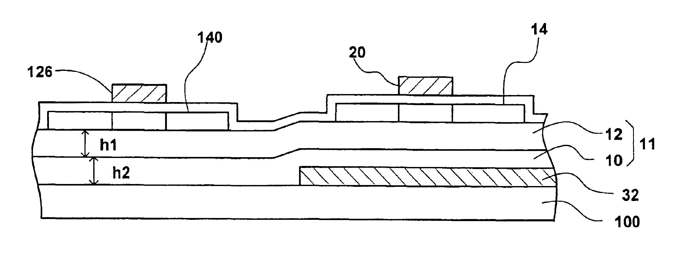
[0037]FIG. 3 schematically shows a structure of a semiconductor device according to the embodiment. As shown in FIG. 3, in the semiconductor device, a metal layer 32 is selectively formed over a portion of a transparent substrate 100 such as glass and a buffer layer 11 is formed covering the metal layer and the entire substrate. The buffer layer 11 has a multi-layer structure of a silicon nitride film 10 and a silicon oxide film 12. In the region where the metal layer 32 is formed, a first polycrystalline silicon film 14 is formed on the buffer layer 11, and a first thin film transistor having the first polycrystalline silicon film 14 as the active layer is formed. In the region where the metal layer 32 is not formed, on the other hand, the buffer layer 11 is formed directly over the substrate 100 and a sec...


PUM


Abstract

In an active matrix type display having built-in drivers, a metal layer is formed over a portion of a transparent substrate and a buffer layer is provided over both the region where the metal layer is formed and over the region where the metal layer is not formed. Above the buffer layer, a first polycrystalline silicon film is provided over the region where the metal layer is formed and a second polycrystalline silicon film is provided over the region where the metal layer is not formed. A buffer layer with sufficient thickness and thermal capacity can provide sufficient distance between the active layers and the lower metal layer to alleviate thermal leakage caused by the metal layer. A first polycrystalline silicon film and a second polycrystalline film each having a proper grain size can be obtained through laser annealing applied under the same conditions on an amorphous silicon film formed over the buffer layer.

Description

CROSS-REFERENCE TO RELATED APPLICATIONS[0001]This application is a continuation application of U.S. patent application Ser. No. 10 / 112,929, filed on Mar. 28, 2002 now U.S. Pat. No. 6,621,103, which is herein incorporated by reference in its entirety.BACKGROUND OF THE INVENTION[0002]1. Field of the Invention[0003]The present invention relates to a lower layer structure for a polycrystalline semiconductor layer, and in particular to a lower layer structure for a polycrystalline silicon active layer of a thin film transistor (hereinafter referred to as a “TFT”) of an active matrix type display.[0004]2. Description of the Related Art[0005]Because the thickness, size, and weight of flat panel displays such as liquid crystal displays (hereinafter referred to as“LCDs”) can be reduced and the flat panel displays have low power consumption, LCDs or the like are now widely used as displays for various devices such as, for example, portable information devices. LCDs having a thin film transist...

Claims


Application Information

Patent Timeline
IPC IPC(8): H01L21/00H01L21/20H01L21/36H01L21/84G02F1/1368G09F9/30H01L21/336H01L21/77H01L27/12H01L29/786
CPCH01L27/12H01L27/1281H01L29/78603H01L29/786
Inventor YAMADA, TSUTOMU
Owner SANYO ELECTRIC CO LTD
Why Eureka
Try Eureka