Gate electrode dopant activation method for semiconductor manufacturing including a laser anneal

a laser anneal and dopant activation technology, applied in the direction of basic electric elements, electrical equipment, semiconductor devices, etc., can solve the problems of thermal budget limitation, degrade device performance and reliability, and the difficulty of producing ultra shallow source/drain junctions

Active Publication Date: 2006-07-18
APPLIED MATERIALS INC
View PDF87 Cites 27 Cited by
  • Summary
  • Abstract
  • Description
  • Claims
  • Application Information

AI Technical Summary

Problems solved by technology

Conventional processes include a rapid thermal annealing process which has a thermal budget limitation.
For example, temperatures higher than 1050° C. are undesirable since boron penetrates through the gate dielectric material to degrade device performance and reliability.
Ultra shallow source / drain junctions are becoming more challenging to produce as junction depth is required to be less than 30 nm for sub-100 nm CMOS (complementary metal-oxide semiconductor) devices.
Conventional doping by implantation followed by thermal post-annealing is less effective as the junction depth approaches the size of 10 nm, since thermal post-annealing causes enhanced dopant diffusion.
Dopant diffusion may contaminate nearby layers and cause failure of the device.
Activating the polysilicon gate electrode without causing dopant diffusion is a major challenge for front end of line (FEOL) processing.
The balance becomes more difficult to maintain as device makers try to overcome poly-depletion.
Conventional thermal processes are not capable of annealing such as small substrate feature without provoking dopant diffusion.
In addition, preventing dopant penetration and use of thermally sensitive high-k materials requires low thermal budget activation anneal.
Laser annealing technology produces transient temperatures near the silicon melting point within a few milliseconds, which results in high dopant activation with little dopant diffusion.
However, laser anneal temperatures that melt the silicon has been shown to cause polycrystalline grain size growth which have been shown to results in device yield loss.

Method used


Image

  • Gate electrode dopant activation method for semiconductor manufacturing including a laser anneal
  • Gate electrode dopant activation method for semiconductor manufacturing including a laser anneal
  • Gate electrode dopant activation method for semiconductor manufacturing including a laser anneal

Examples


Embodiment Construction

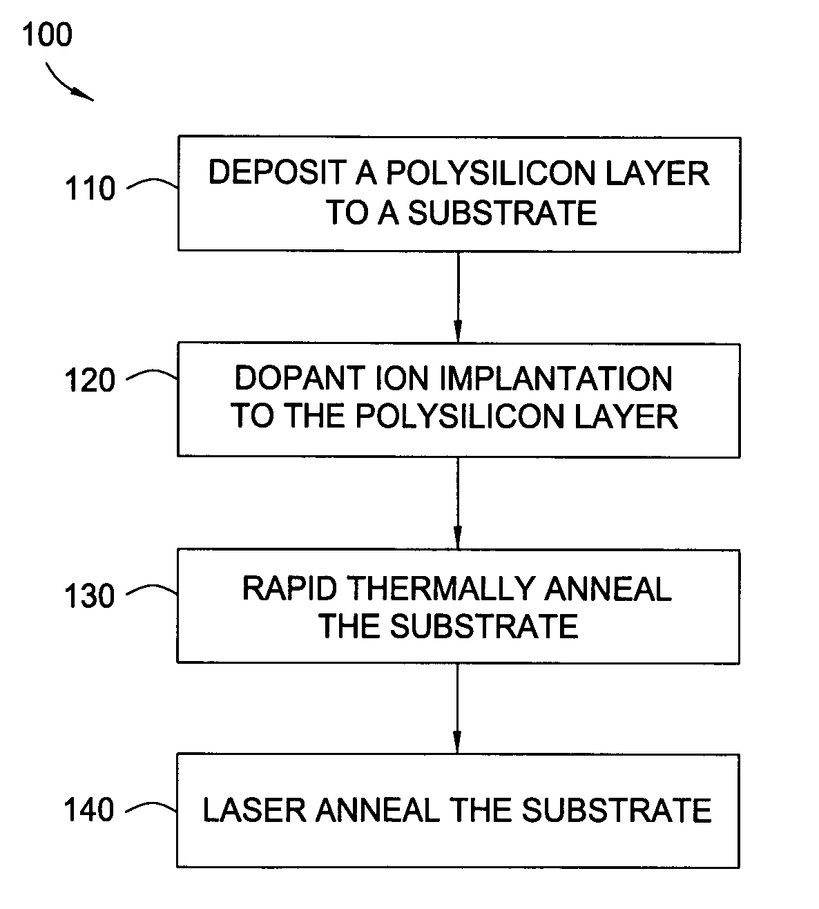
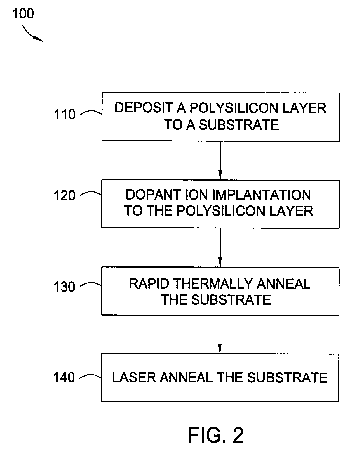
[0017]The present invention teaches methods for forming a doped polycrystalline silicon layer onto a dielectric material, such as silicon dioxide, silicon oxynitride or a high dielectric constant material. Generally, the polycrystalline layer is doped by ion implantation, thermally annealed, such as with a rapid thermal annealing (RTA) process, and subsequently laser annealed to activate the dopants by a dynamic surface anneal (DSA) process.

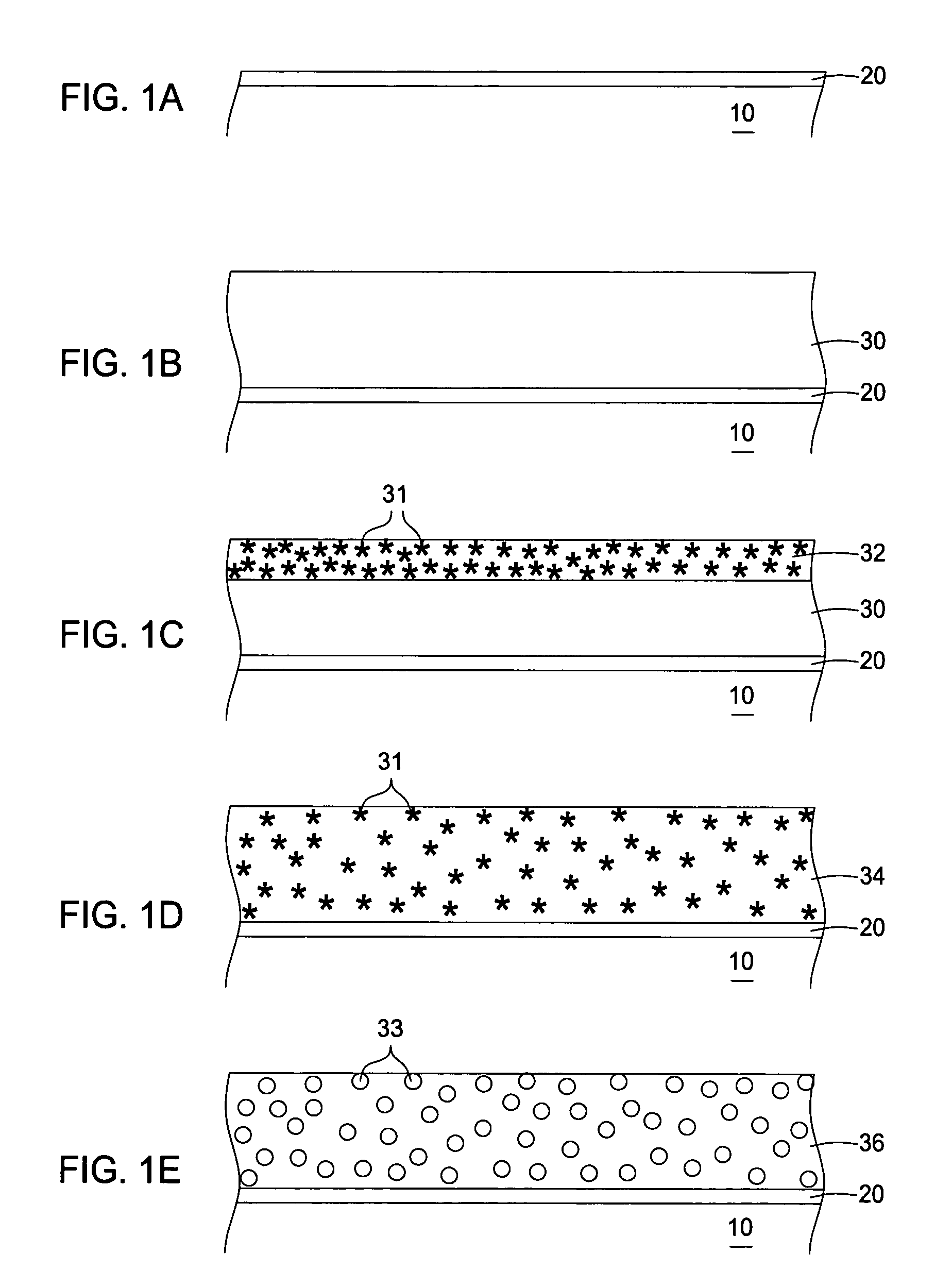
[0018]FIGS. 1A–1E show a cross-sectional view of a gate stack structure progressing through processes disclosed in the present invention. FIG. 1A depicts a dielectric layer 20 disposed on a substrate 10, such as a silicon substrate used in semiconductor processes. In one example, substrate 10 may be a 300 mm p-type silicon substrate doped with boron to resistivity from about 15 Ω-cm to about 20 Ω-cm and is usually pre-cleaned with a conventional pre-gate clean prior to the deposition of dielectric layer 20.

[0019]Dielectric layer 20 may be deposit...


PUM

PropertyMeasurementUnit
temperatureaaaaaaaaaa
timeaaaaaaaaaa
temperatureaaaaaaaaaa

Abstract

In one embodiment, the invention generally provides a method for annealing a doped layer on a substrate including depositing a polycrystalline layer to a gate oxide layer and implanting the polycrystalline layer with a dopant to form a doped polycrystalline layer. The method further includes exposing the doped polycrystalline layer to a rapid thermal anneal to readily distribute the dopant throughout the polycrystalline layer. Subsequently, the method includes exposing the doped polycrystalline layer to a laser anneal to activate the dopant in an upper portion of the polycrystalline layer.

Description

BACKGROUND OF THE INVENTION[0001]1. Field of the Invention[0002]Embodiments of the invention generally relate to the field of semiconductor manufacturing processes, more particular, to methods for dopant activation within silicon-containing films forming semiconductor devices, such as gate electrodes.[0003]2. Description of the Related Art[0004]As smaller transistors are manufactured, thinner gate dielectric material is needed to enhance device performance. However, the carrier depletion contributes about 4 Å to inversion oxide thickness gate electrode material, such as p-type polysilicon doped with boron or n-type polysilicon doped with arsenic and / or phosphorous. Reducing the poly-depletion has become critical to maintain the device performance. Conventional processes include a rapid thermal annealing process which has a thermal budget limitation. For example, temperatures higher than 1050° C. are undesirable since boron penetrates through the gate dielectric material to degrade d...

Claims


Application Information

Patent Timeline
Patent Type & Authority Patents(United States)
IPC IPC(8): H01L21/336H01L21/22H01L21/3205H01L21/38H01L21/4763H01L21/268H01L21/28H01L21/324
CPCH01L21/268H01L21/324H01L21/28035
Inventor MA, YIAHMED, KHALED Z.CUNNINGHAM, KEVIN L.MCINTOSH, ROBERT C.MAYUR, ABHILASH J.LIANG, HAIFANYAM, MARKLEUNG, TOI YUE BECKYOLSEN, CHRISTOPHERWANG, SHULINFOAD, MAJEEDMINER, GARY EUGENE
Owner APPLIED MATERIALS INC
Why Eureka
Try Eureka